Get a Quote
OUR BLOG
Focus on the latest articles that cover topics ranging from the latest technologies to best practices and industry news for PCB.
Oct 19, 2026
PCB thickness is often treated as a simple mechanical specification, but it can have a direct effect on manufacturing cost. A standard PCB may use a common thickness such as 1.6 mm, while other applications may require 0.8 mm, 1.0 mm, 1.2 mm, 2.0 mm, or even thicker constructions. Changing the thickness does not simply […]
Oct 13, 2026
Oct 07, 2026
19
Oct
PCB surface finish affects more than solderability. HASL, lead-free HASL, ENIG, OSP, immersion silver, and other finishes have different processing costs, applications, and limitations. Choosing the appropriate finish can help control PCB manufacturing cost without compromising assembly requirements.
13
Copper weight directly affects PCB material usage, etching, plating, thermal performance, and manufacturing cost. This article explains how 1 oz, 2 oz, and heavy copper change PCB pricing and when additional copper is actually necessary.
07
PCB tooling costs are often included in the manufacturing quotation without much explanation. Depending on the PCB structure and order quantity, tooling can include drilling, routing, fixtures, electrical test equipment, and production setup. This article explains what PCB tooling costs mean, when they are charged, why prototype orders can be affected more strongly, and how to evaluate tooling costs when comparing PCB quotations.
02
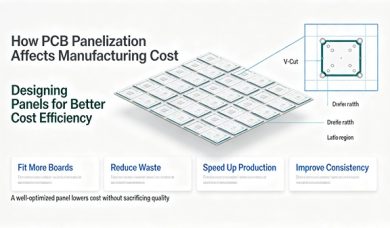
PCB panelization determines how efficiently individual boards are arranged on a manufacturing panel. A well-planned panel can reduce material waste, improve production efficiency, and lower the effective cost per PCB. This article explains how board size, shape, spacing, routing, V-grooves, tooling rails, and production quantity influence panelization and overall PCB cost.
30
Sep
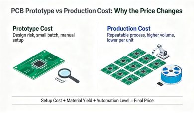
PCB prototype pricing can be much higher per unit than production pricing, even when the board specification remains unchanged. The difference comes from setup costs, engineering preparation, panel utilization, purchasing volume, testing, and production efficiency. This article explains how prototype and production PCB costs differ and how to decide when a project is ready to move from prototype builds to volume production.
24
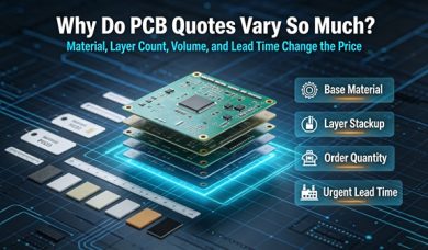
PCB quotations for the same design can sometimes differ significantly. The difference does not always mean that one manufacturer is more expensive. Material specifications, stackup, copper weight, surface finish, tolerances, testing, quantity, and lead time can all change the final price. This article explains how to compare PCB quotes on an equivalent technical basis and identify the reasons behind major price differences.
18
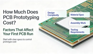
PCB prototype pricing is often much higher per board than production pricing because setup, engineering, tooling, and material costs are spread across a small quantity. This article explains what affects prototype PCB cost and how engineers can reduce unnecessary expenses without compromising the validation process.
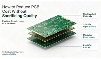
Reducing PCB cost does not necessarily mean choosing cheaper materials or removing quality controls. The biggest savings often come from eliminating unnecessary manufacturing complexity before production. This article explains practical ways to lower PCB cost through stackup optimization, material selection, panelization, via design, tolerances, surface finish, and production planning while maintaining reliability.
08
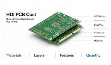
HDI PCBs can reduce board size and support fine-pitch components, but their manufacturing process is more complex than conventional multilayer fabrication. The cost depends heavily on the HDI structure, microvias, sequential lamination, materials, layer count, board size, and production quantity. This article explains where HDI costs come from and how to decide whether the additional complexity is justified.
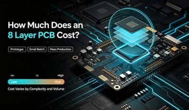
An 8 layer PCB provides significantly more routing and reference-plane options than a 4 or 6 layer board, making it suitable for dense and high-speed designs. The additional layers also increase material consumption and fabrication complexity. This article explains the main cost drivers of 8 layer PCBs and how engineers can control cost without compromising signal integrity or reliability.
29
Aug
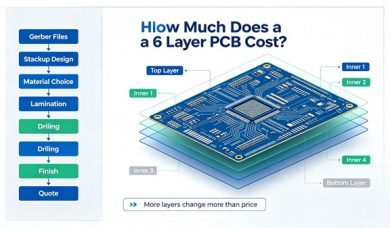
A 6 layer PCB provides more routing and power distribution options than a 4 layer board, but the additional layers also introduce more lamination and fabrication requirements. This article explains the main factors behind 6 layer PCB pricing and when moving from 4 to 6 layers can actually make engineering and production more practical.
Load More
Layers 1 Layers 2 Layers 4 Layers 6 Layers 8 Layers 10 Layers 12 Layers 14 Layers
Dimensions (mm)
Quantity 5 10 15 20 25 30 35 40 50 75 100 100+
Thickness 0.4mm 0.6mm 0.8mm 1.0mm 1.2mm 1.6mm 2.0mm 2.4mm
Quantity
Number of Unique Parts
SMT Pads
Thru-Holes

 EN
EN  PT
PT  AR
AR  DE
DE  FR
FR  ES
ES