Professional PCB Manufacturing Solutions
One-Stop PCB Manufacturing
Core
Support for Every Industry
From aerospace to smart homes, our PCB technology empowers your products to lead the market
0
Years of Experience
0
Industries Served
0
Quality Yield Rate
0
Global Clients
Industries We Serve
Covering 12 Core Industries
Our PCB solutions meet the strictest requirements across industries

Aerospace PCB
Extreme Reliability
High-reliability PCBs designed for aerospace and
defense applications.
- AS9100 & MIL-STD certified
- Wide temperature range (-55C to 125C)
- Heavy copper & thick backplanes

Industrial Control PCB
Stable & Efficient
Rugged PCBs built for industrial automation and
control systems.
- Anti-vibration & shock resistant
- High-temperature materials
- Conformal coating available
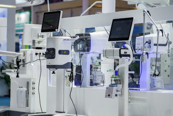
Medical PCB
Precise & Safe
Ultra-precise PCBs for medical devices meeting
highest safety standards.
- ISO 13485 certified process
- HDI & micro-via technology
- Bio-compatible materials

Automotive PCB
Durable & Robust
Automotive-grade PCBs designed for extreme vehicle
conditions.
- IATF 16949 certified
- Heavy copper for power modules
- Thermal management solutions

Consumer Electronics PCB
Thin & High-Performance
Compact, high-density PCBs for smartphones,
tablets, wearables.
- HDI with blind & buried vias
- Ultra-thin substrates
- High-speed signal integrity

AI Smart Care
Intelligent & Caring
Advanced PCBs powering AI-driven health monitoring
devices.
- Low-power sensor integration
- Wireless connectivity (BLE/Wi-Fi)
- Miniaturized design

Smart Home PCB
Connected & Seamless
PCBs for smart home devices enabling IoT
connectivity.
- Multi-protocol RF design
- Compact form factors
- Low power consumption

IOT PCB
Everything Connected
IoT-optimized PCBs with integrated wireless
modules.
- Embedded antenna design
- Multi-layer RF capability
- Extreme miniaturization
Semiconductor PCB
Precision & Cutting-Edge
High-precision PCBs for semiconductor testing
equipment.
- Ultra-fine pitch capability
- Ceramic & advanced substrates
- Test socket boards

Communication PCB
High-Speed & Stable
High-frequency PCBs for 5G, telecom infrastructure.
- Low Dk / Df materials
- Impedance control +/-5%
- 10+ Gbps signal speeds
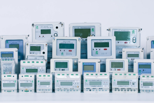
Smart Meter PCB
Accurate & Reliable
PCBs for smart metering with high-precision
measurement.
- High voltage isolation
- Long-term stability (15+ years)
- Wireless communication ready

Energy Equipment PCB
Efficient & Reliable
Heavy-duty PCBs for solar, wind, battery systems.
- Heavy copper up to 6oz
- High thermal conductivity
- High voltage capability
Core Advantages
Why Choose Us
20 years of industry expertise, forging excellence in every board
01
Fast Turnaround
24-hour prototype, 3-7 day mass production. Flexible to meet your urgent order needs.
02
Quality Guaranteed
ISO 9001, IATF 16949, AS9100 certified. End-to-end quality management.
03
Expert Engineering Support
Senior team providing DFM review, stackup design, impedance control.
04
Global Delivery
DHL, FedEx, UPS worldwide shipping. Serving 150+ countries with reliable logistics.
Technical Capabilities
Core Technical Parameters
Advanced manufacturing capabilities to meet your diverse requirements
| Parameter | Standard Capability | Advanced Capability |
|---|---|---|
| Layers & Thickness | ||
| Layer Count | 1-16 Layers | Up to 40 Layers |
| Finished Board Thickness | 0.4-3.2 mm | 0.2-6.0 mm |
| Inner Layer Copper | 0.5-1 oz | Up to 3 oz |
| Outer Layer Copper | 0.5-2 oz | Up to 6 oz |
| Trace & Spacing | ||
| Minimum Trace Width | 0.1 mm (4 mil) | 0.075 mm (3 mil) |
| Minimum Trace Spacing | 0.1 mm (4 mil) | 0.075 mm (3 mil) |
| Impedance Tolerance | ±10% | ±5% |
| Impedance Control Range | 50-100 Ω | 25-150 Ω |
| Hole & Via | ||
| Minimum Drilled Hole (Mechanical) | 0.2 mm | 0.15 mm |
| Minimum Laser Via | 0.1 mm | 0.075 mm |
| Hole Position Tolerance | ±0.05 mm | ±0.025 mm |
| Max Aspect Ratio | 10:1 | 16:1 |
| Dimensions & Tolerance | ||
| Max Board Size | 500 x 600 mm | 610 x 1200 mm |
| Outline Tolerance | ±0.2 mm | ±0.1 mm |
| Bow & Twist | <1.0% | <0.7% |
| Solder Mask Registration | ±0.075 mm | ±0.05 mm |
Customer Value
Why Customers Choose Us
We don't just deliver PCBs - we deliver long-term value

ISO Certified Factory
√
One-Stop Solution
Full-chain service from design to assembly, reducing your communication costs.
√
Flexible Production
From small-batch prototypes to large-scale mass production, consistent quality at every volume.
√
Cost Optimization
Our engineers provide DFM suggestions at the design stage to help reduce manufacturing costs.
√
24/7 Support
Fast response around the clock, our dedicated team is always ready to solve technical challenges.
√
Strict IP Protection
Comprehensive intellectual property protection system ensures your design information is secure.
FAQ
Frequently Asked Questions
Find answers to common questions about our PCB services
How do I get a PCB
quote?
Submit your Gerber files, PCB specifications, and quantity
requirements through our Get Quote button. Our sales team will provide a detailed quote
within 24 hours.
What is the minimum order
quantity?
We support orders starting from just 1 piece. Whether it is prototype
or mass production, we have dedicated channels for small-batch orders.
What is the typical production
lead time?
Standard: double-sided 3-5 days, 4-8 layer 5-7 days. Expedited:
24-hour and 48-hour options available depending on your specifications.
What file formats do you
accept?
We support Gerber RS-274X, ODB++, IPC-2581 standard formats, as well
as native files from Altium Designer, KiCad, Eagle, and other EDA tools.
How do you ensure product
quality?
Every PCB undergoes AOI inspection, electrical testing, and final
quality audit. We provide complete test reports with every shipment. ISO 9001 and IATF 16949
certified.
What surface finishes are
available?
We offer multiple surface finish options: HASL (Lead-Free/Leaded),
ENIG (Immersion Gold), OSP, Immersion Silver, Immersion Tin, Hard Gold (Gold Fingers), and
ENEPIG.