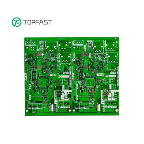
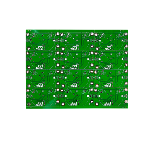
HDI PCB Manufacturing Services
Topfast specializes in manufacturing high-density interconnect (HDI) PCBs with precision-engineered solutions, including blind vias, buried vias, microvias, and sequential lamination.
Leveraging cutting-edge production processes, we deliver superior performance, exceptional reliability, and compact designs tailored to meet the most demanding electronic applications.
Ultra-high density wiring
Utilizes laser microvia and blind/buried via technology
Advanced manufacturing processes
High-precision laser drilling, sequential lamination, ultra-thin dielectric materials
High reliability and stability
Strict quality control, high TG materials (Tg ≥ 170°C)
Fast delivery & cost optimization
Rapid prototyping for small to medium batches, cost reduction through large-scale production
Advanced HDI technology enables smaller, faster, and more reliable PCBs
Why Choose HDI PCBs?
High-Density Interconnect technology for advanced electronic applications
High Wiring Density
Utilizes microvia and blind/buried via technology to achieve a more refined circuit layout with increased component density.
Multi-layer Stacking
Employs any-layer HDI or sequential lamination technology to improve signal transmission efficiency and reduce interference.
Compact & Lightweight
Ideal for space-constrained devices including smartphones, tablets, and wearable technology.
High-Frequency Performance
Optimized signal integrity for demanding applications like 5G communication and high-end server infrastructure.
HDI PCB Material Selection
In high-density interconnect (HDI) PCB design, material selection directly impacts signal integrity, thermal reliability, and long-term stability. Topfast combines industry standards with customer requirements to optimize material solutions.
01
Decomposition Temp (Td)
Maintains stability during reflow soldering processes (250-300°C)
02
Dielectric Constant (Dk)
Reduces signal delay for 5G/mmWave applications and high-speed data.
03
Glass Transition (Tg)
Prevents board deformation in multilayer stacks during thermal cycles.
04
Dissipation Factor (Df)
Minimizes signal loss in ultra-high speed and radio frequency applications.
05
Thermal Expansion (CTE)
Ensures reliability of solder joints and vias during extreme thermal stress.
06
Copper & Surface
Enables ultra-fine line circuitry and reduces high-frequency skin effects.
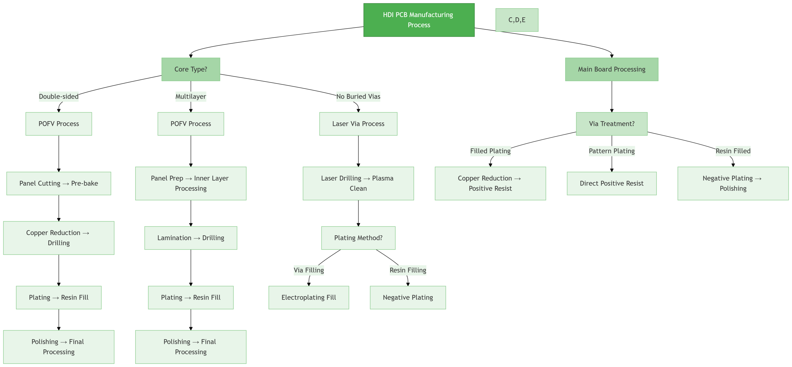
HDI PCB Manufacturing Process
A precision-driven workflow ensuring every micron meets industry standards.
Frequently Asked Questions
How reliable are HDI PCBs in the long term?
We strictly enforce every step of the process and are committed to providing our customers with high-quality products via rigorous testing and quality management systems including AOI, X-Ray, and Flying Probe testing.
Do you provide DFM advice for new HDI designs?
Yes. Our engineering team provides comprehensive DFM (Design for Manufacturing) feedback to optimize cost, improve yield, and ensure the design is production-ready before starting manufacturing.
Why are HDI PCBs more expensive than ordinary PCBs?
HDI requires specialized equipment (laser drilling), multi-stage sequential lamination, and higher-grade materials like BT resin or high-TG substrates to manage density and heat effectively.
What is the delivery time for HDI PCBs?
Typically 7-10 days for prototypes. The extra time compared to standard multilayer PCBs accounts for complex repeated drilling and lamination cycles necessary for high precision.
Does your factory have actual HDI experience?
Topfast specializes in thin-core HDI with extensive experience in 1+N+1 to Any-Layer stacks for medical, automotive, and high-end consumer sectors globally.
What are your minimum trace and hole limits?
We achieve 40μm line width/spacing and 50μm laser via diameters using world-class VCP and LDI equipment to meet ultra-fine design requirements.
Can you rush the production for urgent projects?
Yes. If materials are in stock, we offer 24-48 hour rapid prototyping for urgent HDI projects with a reasonable expedite fee for prioritized scheduling.
What certifications do you hold for HDI?
We are ISO 9001, ISO 14001, and UL certified. All products comply with IPC-6012 Class 2 or 3 and RoHS environmental standards for global compliance.
Still have questions?
Check All Help CenterIndustry Applications
Our HDI solutions power mission-critical electronics across diverse global sectors.