High-Density Interconnect (HDI) printed circuit boards (PCBs) are specialized PCBs designed for applications requiring high component density, miniaturization, and improved signal integrity. HDI PCBs are commonly used in smartphones, laptops, medical devices, and other electronics where space and performance are critical.
As electronic devices shrink, the demand for High-Density Interconnect (HDI) technology surges. While conventional boards rely on mechanical drilling, the HDI PCB manufacturing process utilizes laser microvias and sequential lamination to achieve ultra-fine circuit density. This guide dives into the critical stages—from mSAP (modified Semi-Additive Process) to advanced reliability testing—ensuring your design meets IPC-Class 3 standards.
Table of Contents
Solution for HDI PCB Manufacturing – Unveiling Intricate Steps for Superior Performance and Density
Design and Layout
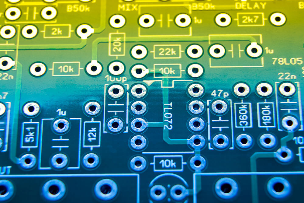
Like any PCB, the HDI PCB manufacturing process starts with design and layout using specialized PCB design software. Designers carefully plan the component placement, routing, and the number of layers required to achieve the desired density. HDI PCBs often use microvias and blind vias to connect layers.
Material Selection
The choice of materials is critical for HDI PCBs. Advanced materials with low dielectric constants, such as high-performance laminates or polyimide, are often used to enable high-frequency signal transmission and reduce signal loss.
Layer Stackup
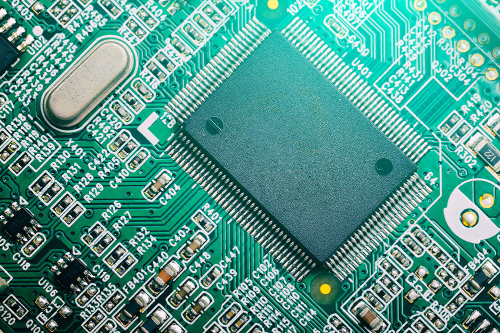
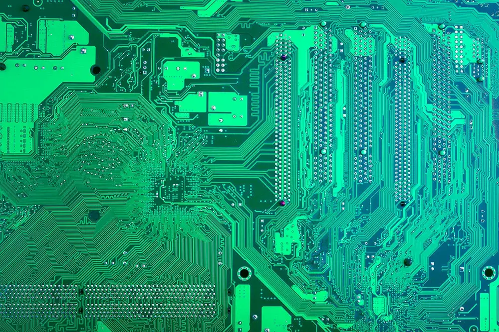
HDI PCBs typically have multiple layers (e.g., 4, 6, 8, or more) to accommodate densely packed components. The layer stackup specifies the number of signal layers, power and ground planes, and any buried or blind vias.
Laser Drilling
Laser drilling is a key step in HDI PCB manufacturing. High-precision lasers create tiny holes, known as microvias, which are used to connect different layers within the PCB. Microvias are essential for achieving high component density and reducing signal path length.
At Topfast, we utilize UV and CO2 Laser Drilling to create microvias with an aspect ratio of $0.75:1$. For high-speed applications, we implement VIPPO (Via-in-Pad Plated Over) technology. This involves filling the vias with conductive or non-conductive epoxy and capping them with copper to provide a flat, solderable surface directly on the pad.
Sequential Lamination
The PCB is built up layer by layer through sequential lamination. Each layer is individually etched, and additional copper and dielectric material are added as needed. The microvias are connected and plated during this process. The complexity of an HDI board is defined by its Build-up structure (e.g., 1+N+1, 2+N+2). Each additional ‘stack-up’ layer requires a separate lamination cycle. To maintain signal integrity, we recommend using high-Tg materials like Megtron 6 to minimize thermal stress during these multiple cycles.
Copper Plating
Copper is electroplated onto the PCB’s surface and into the microvias to create conductive traces and connections. Copper plating ensures low impedance paths for signals and power distribution.
Solder Mask Application
A solder mask is applied to cover and insulate the copper traces, leaving only the areas for component attachment exposed. Solder mask protects the PCB from environmental factors and defines soldering pads.
Surface Finish
A surface finish is applied to the exposed copper surfaces to enhance solderability and protect against oxidation. Common surface finishes include ENIG (Electroless Nickel Immersion Gold), OSP (Organic Solderability Preservatives), and immersion tin.
Silkscreen Printing
Component labels, reference designators, and other markings are printed onto the PCB’s surface to aid in component placement and assembly.
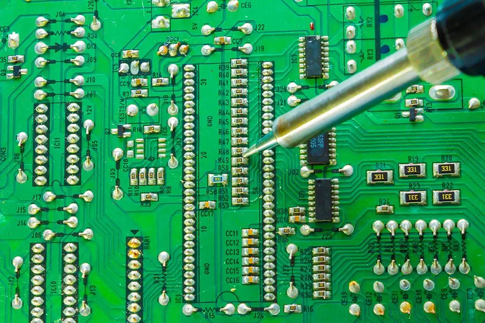
Quality Control
Rigorous quality control processes are implemented throughout the manufacturing process. This includes inspections, electrical testing, and impedance measurements to ensure the HDI PCB meets design specifications. A Closer Look into Quality Control within PCB Manufacturing.
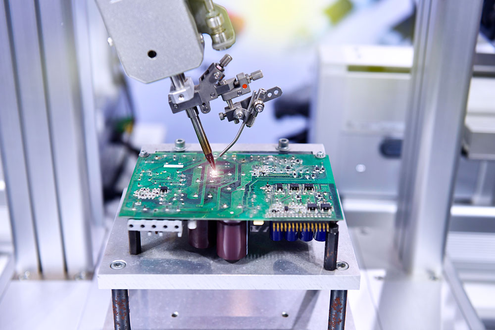
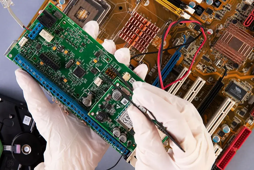
Assembly
After manufacturing, electronic components are assembled onto the HDI PCB. Advanced assembly techniques, such as surface mount technology (SMT), are often used to place and solder components with precision.
Testing
The completed HDI PCBs undergo functional testing to ensure they meet performance and functionality requirements. This may include signal integrity testing, electrical testing, and automated optical inspection (AOI).
Differences Between the HDI Manufacturing Process and Conventional PCB Manufacturing
High-Density Interconnect (HDI) manufacturing processes differ significantly from traditional printed circuit board (PCB) manufacturing processes due to the specialized techniques and design considerations required to achieve higher component density and miniaturization:
Layer Count and Complexity
Traditional PCBs typically consist of two or four layers, while HDI PCBs often have six or more layers.
HDI PCBs can incorporate multiple layers of fine-pitch components, high-speed signal traces, and ground/power planes, allowing for complex and compact designs.
Microvias and Blind/Buried Vias
HDI PCBs extensively use microvias, which are tiny holes drilled with precision lasers, to establish connections between layers. These microvias are much smaller than the through-holes used in traditional PCBs.
Blind vias connect an outer layer to one or more inner layers, while buried vias connect inner layers without penetrating the outer layers. Traditional PCBs typically use through-hole vias.
Advanced Materials
HDI PCBs often employ advanced materials with low dielectric constants to minimize signal loss and achieve high-frequency performance.
Traditional PCBs may use standard FR-4 materials, which may not be suitable for high-density or high-speed applications.
Laser Drilling
HDI PCB manufacturing relies on precise laser drilling to create microvias, whereas traditional PCBs use mechanical drilling for larger through-hole vias.
Sequential Lamination
HDI PCBs are built up layer by layer through sequential lamination, allowing for the controlled addition of copper and dielectric material on each layer.
Traditional PCBs are typically manufactured using a single lamination process.
Copper Plating
Copper plating in HDI PCBs is critical for creating fine traces and connections, often requiring advanced plating techniques.
Traditional PCBs may use standard copper plating methods without the need for as much precision.
Solder Mask and Surface Finish
Solder masks in HDI PCBs are applied to insulate the smaller and denser traces and to define soldering pads for tiny components.
Traditional PCBs use solder masks primarily for insulation and to define soldering areas.
Surface finishes on HDI PCBs are carefully selected for improved solderability and signal integrity.
Traditional PCBs may use less advanced surface finishes, such as HASL (Hot Air Solder Leveling).
Component Assembly
Component assembly for HDI PCBs often involves advanced techniques like surface mount technology (SMT) due to the smaller component sizes and higher component densities.
Traditional PCBs may use through-hole component assembly methods more frequently.
Testing and Inspection
HDI PCBs undergo more rigorous testing for signal integrity, impedance control, and microvia reliability.
Traditional PCBs may have less stringent testing requirements.
Design Considerations
HDI PCBs require meticulous attention to signal integrity, impedance matching, and EMI/RFI mitigation due to the higher frequency signals and compact layouts.
Traditional PCBs may prioritize different design aspects depending on the application.
HDI PCB manufacturing requires specialized equipment and expertise due to the high component density and miniaturization demands. The precision and attention to detail in each step of the process are crucial for ensuring the final product meets the requirements for high-density and high-performance electronic applications.
How to Optimize Your Design for the HDI Manufacturing Process
- Define Your Stack-up:
Choose between staggered or stacked vias based on your density requirements.
- Select Advanced Materials:
Use low-Dk/Df laminates for high-frequency performance.
- Implement DFM Rules:
Ensure trace width and spacing (e.g., $3/3\text{mil}$) align with Topfast’s HDI Manufacturing Capabilities.
- Final DRC Check:
Validate microvia aspect ratios to prevent plating failures.
Frequently Asked Questions about HDI Manufacturing
A: Laser vias are much smaller (typically $0.1\text{mm}$ or less), allowing for significantly higher component density and better signal integrity in compact designs.
A: Due to the sequential lamination cycles, HDI boards typically take 3-5 days longer than standard multi-layer PCBs.
Mastering the HDI PCB manufacturing process is essential for modern electronics. At Topfast, our engineering team reviews every design to ensure manufacturability. Last Updated: March 11, 2026 | Reviewed by Topfast Technical Department. Ready to start? Get an Online Quote for your HDI project now.