In the complex world of printed circuit board (PCB) design, gaining proficiency in multilayer PCB designs becomes inevitable. This comprehensive article delves into the nuanced aspects that every designer must familiarize themselves with, for flawless multilayer PCB designs. From understanding the basics of multilayer PCBs, making appropriate layer stackup choices, and ensuring signal integrity, to the strategic management of power and ground planes, thermal factors, component placement, and routing – readers will get a well-rounded view. We also delve into crucial manufacturing considerations, arming you with the knowledge to avoid costly mistakes. Buckle up as we journey through the intriguing intricacies of multilayer PCB design.
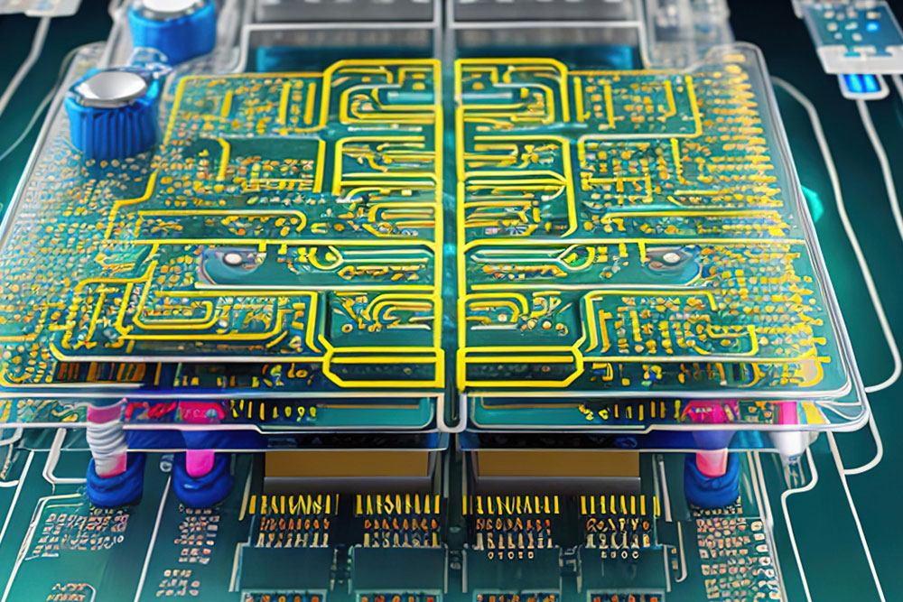
Table of Contents
Multilayer PCB Basics
Navigating through the realm of multilayer PCB design commences with a clear understanding of its basics. Multilayer PCBs consist of more than two conductive copper layers positioned between layers of insulating material. The number of layers may vary, lending versatility to the board’s functionality, but it also adds to the complexity. Each layer interacts with the others, influencing attributes like signal integrity and thermal management. Fundamental to engineering multilayer PCBs is the comprehension of through-holes, vias, blind and buried vias that establish connections across the layers. As an essential foundation, these basics not only help in developing efficient boards but also foster informed decision-making regarding layer stackup selection, component placement, and more. Understanding the fundamentals can be the difference between efficient design and an expensive paperweight.
Selecting the Right Layer Stackup
Selecting the right layer stackup is a fundamental, yet intricate stage in multilayer PCB design. The choice of layer stackup not only affects the board’s functionality, but also its manufacturability and cost. The process involves a strategic balance of electrical needs, thermal performance, and physical constraints of the PCB. Different applications will require different stackups; for instance, high-speed designs may lean towards more signal layers, while more power-intensive applications may prioritize power and ground planes. Understanding the mechanical stress on the board, along with signal integrity requirements, and electromagnetic compatibility is pivotal in layer stackup selection. As designers, cultivating an in-depth knowledge of this aspect of design can pave the way to creating reliable, functional, and cost-efficient multilayer PCBs.
Signal Integrity Considerations
In the realm of multilayer PCB design, signal integrity considerations play a pivotal role. This involves ensuring that the signals transmitted across the PCB face minimal disruption and degradation. As designs grow more complex, and as frequencies and speeds increase, the challenge to maintain signal integrity escalates. Aided by simulation tools, designers have the task to balance signal paths, manage crosstalk, handle impedance mismatches, and mitigate electromagnetic interference (EMI). Proper consideration of factors such as trace widths, layer stackup, routing topology, and ground plane usage can significantly enhance signal quality. To maintain signal integrity in multilayer PCB designs is to effectively tame the complexities faced, enabling smoother operation and increased system performance.
Power and Ground Planes
Ensuring effective power and ground planes is an integral part of optimizing multilayer PCB. These planes serve as the cornerstone for maintaining the stability and performance of your PCB, providing succinct paths for current flow and reducing the loop area. Efficiently designed power and ground planes not only contribute to improving the signal integrity but also substantially minimize electromagnetic interference (EMI). Therefore, careful planning in the allocation and arrangement of these planes can have a profound impact on the functionality of your design. Bear in mind, managing the balance between the power and ground planes while simultaneously considering other factors such as thermal management can be complex. In this section, we’ll dissect the most pertinent considerations for designing effective power and ground planes.

Thermal Management
Navigating the realm of thermal management in multilayer PCB design is no easy task, yet it is vital for the long-term functionality and reliability of your PCB. Inadequate thermal strategies can lead to overheating, component failure, and even board warping. By employing techniques such as using thermal vias to dissipate heat and selecting the right materials for high-temperature environments, you can promote efficient heat distribution. Aligning power and ground planes can also offer a thermal path, whereas planning component placement with heat production in mind can prevent localized hotspots. Acknowledging thermal implications from the get-go ensures a robust design that can withstand even the harshest thermal conditions.
Component Placement and Routing
Component placement and routing represent a critical phase in multilayer PCB design where precision and intelligent strategy play a crucial role. Ensuring appropriate component placement is more than just about making the board look orderly—it’s about optimizing board performance, minimizing electromagnetic interference, and increasing board density. Careful attention must also be given to routing, where signal paths are created. It influences signal integrity and significantly impacts the speed and reliability of the board’s performance. Mastery of these factors involves understanding the interplay between placement and routing to navigate the complex trade-offs and challenges posed. This section will enrich your understanding and provide actionable insights to fine-tune these complex aspects of multilayer PCB design.
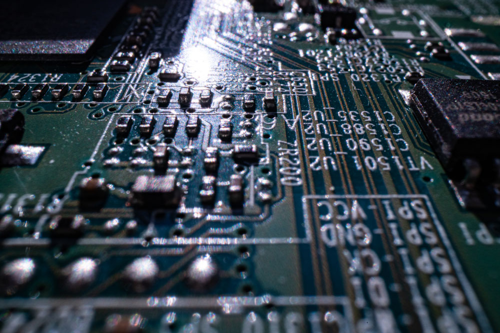
Manufacturing Considerations
An integral part of the multilayer PCB design process is taking into account manufacturing considerations to ensure the smooth transition of your design from conception to the final product. It’s critical to have a deep understanding of the specific tolerances and capabilities of your manufacturer from the early design stages. Key considerations include materials, panel sizes, aspect ratios, trace widths, via sizes, and surface finishes. The layout should also consider the manufacturing assembly processes, such as parts placement, soldering, and testing. Furthermore, closely understanding the Design for Manufacture (DFM) rules helps to minimize potential fabrication issues, reducing the risk of costly reruns or product failures. Observing these aspects can maximize production efficiency, product reliability, and ultimately result in a successful multilayer PCB design.