
Drilling is one of the fundamental processes in PCB fabrication, but the drilling requirements of a board can have a surprisingly large effect on manufacturing cost.
A simple two-layer PCB with standard through-holes is relatively straightforward to fabricate.
A high-density multilayer PCB with hundreds of small vias, high aspect-ratio holes, blind vias, buried vias, or microvias requires a much more complex manufacturing process.
The cost difference does not come from drilling alone.
Hole structure can also affect:
- Plating
- Aspect ratio
- Registration
- Laser processing
- Tool wear
- Production time
- Inspection
- Yield
- Stackup design
For this reason, drilling specifications should be considered early in the PCB cost evaluation rather than added as a manufacturing detail after the layout is complete.
Table of Contents
What Makes PCB Drilling Expensive?
Several factors contribute to PCB drilling cost.
The most important include:
- Number of holes
- Minimum hole diameter
- Hole type
- PCB thickness
- Aspect ratio
- Material
- Hole tolerance
- Back drilling
- Laser drilling
- Via filling
- Plating requirements
A board with thousands of conventional through-holes can have a very different cost structure from a board with fewer but much smaller laser vias.
Therefore, hole count alone does not determine drilling cost.
The manufacturing method matters just as much.
Through-Hole Drilling
Through-holes pass completely through the PCB.
They can be used for:
- Component leads
- Mounting holes
- Plated vias
- Mechanical connections
Through-hole drilling is one of the most established PCB fabrication processes.
For standard hole sizes and ordinary board thicknesses, it is generally easier to manufacture than specialized via structures.
However, cost can increase when a board contains a very large number of holes or requires very small mechanical drill sizes.
Why Hole Count Affects PCB Cost
Each drilled hole requires machine time.
A simplified relationship is:
More holes → More drilling operations → Longer production time
But the relationship is not perfectly linear.
The production process also depends on:
- Tool changes
- Hole size distribution
- Panel size
- Board thickness
- Drill speed
- Material
- Machine setup
For example, a board with 2,000 holes using only a few standard drill sizes may be easier to process than a board with 500 holes using many different drill diameters.
The number of unique drill tools can therefore matter as well as the total hole count.
Minimum Hole Size and Cost
Minimum hole diameter is one of the most important drilling specifications.
Large holes are generally easier to drill.
As the hole diameter becomes smaller, manufacturing becomes more sensitive to:
- Drill breakage
- Position accuracy
- Material characteristics
- Tool wear
- Aspect ratio
- Plating quality
For this reason, unnecessarily small mechanical holes can increase PCB fabrication cost.
If a 0.30 mm finished hole can perform the same electrical function as a 0.20 mm hole, the larger hole may provide a more manufacturing-friendly solution.
The actual minimum drill capability depends on the PCB manufacturer and board construction, so the required hole size should be discussed before production.
Finished Hole Size vs Drill Tool Size
An important detail in PCB quotations is the difference between the finished hole size and the drill tool diameter.
The final plated hole can be smaller than the original mechanical drill diameter because copper is deposited during plating.
For example, a design may specify a finished hole diameter rather than the drill diameter.
This distinction should be clearly defined in the fabrication specification.
Otherwise, two manufacturers may interpret the same drawing differently.
When comparing PCB quotations, always confirm whether the stated hole size refers to:
- Finished hole
- Drill diameter
- Plated hole
- Non-plated hole
This can prevent inaccurate price comparisons.
PCB Thickness and Hole Aspect Ratio
Hole aspect ratio is another major factor.
A simplified calculation is:
Aspect Ratio = Board Thickness ÷ Hole Diameter
For example:
- 1.6 mm board / 0.4 mm hole = 4:1
- 1.6 mm board / 0.2 mm hole = 8:1
- 2.0 mm board / 0.2 mm hole = 10:1
The smaller the hole relative to board thickness, the more demanding the fabrication process can become.
High aspect-ratio holes can create challenges for:
- Drilling
- Hole-wall quality
- Copper plating
- Solution circulation
- Reliability
This is why hole size should always be evaluated together with finished board thickness.
For more information on the cost implications of thickness, see PCB Thickness Cost: How Board Thickness Affects Price.
Small Holes Can Increase More Than Drilling Cost
A common mistake is to assume that a small hole only increases the drilling line item.
In reality, small holes can affect several manufacturing processes.
For example, a small plated through-hole may require:
- Precise drilling
- Careful hole-wall preparation
- Reliable copper plating
- Tighter inspection
- Better registration control
If the board uses high-density interconnect structures, additional processes may also be necessary.
The result is a change in the overall fabrication cost rather than simply an additional drilling charge.
Mechanical Vias vs Laser Microvias
Not all vias are drilled in the same way.
Mechanical Vias
Mechanical drilling is commonly used for conventional through-holes and many standard vias.
It is suitable for a wide range of PCB structures.
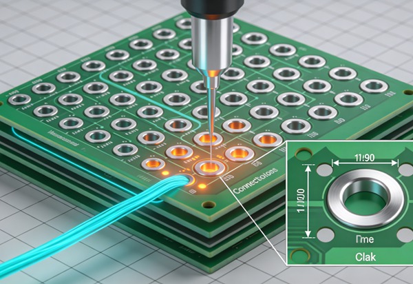
Laser Microvias
Laser drilling is commonly used for very small microvias in HDI structures.
Laser drilling can create much smaller features than conventional mechanical drilling.
However, it also introduces additional process requirements and equipment.
Therefore, microvia structures generally have a different cost structure from conventional through-hole vias.
For high-density designs, the cost of the complete HDI structure should be considered rather than comparing the laser-drilling step alone.
Blind Vias and Buried Vias
Blind and buried vias can increase PCB manufacturing complexity.
Blind Via
A blind via connects an outer layer to one or more internal layers but does not pass through the entire PCB.
Buried Via
A buried via connects internal layers without reaching the outer surface.
These structures can improve routing density, but they require additional manufacturing processes.
Depending on the stackup, they may involve:
- Sequential lamination
- Additional drilling
- Additional plating
- Registration control
- Via filling
As a result, blind and buried vias generally need to be evaluated as part of the overall multilayer manufacturing cost.
Microvia Cost
Microvias are particularly relevant to HDI PCBs.
They are commonly produced using laser drilling and may require additional copper processing.
The cost can be influenced by:
- Via diameter
- Via depth
- Layer structure
- Via density
- Stacked or staggered configuration
- Via filling
- Copper filling
- Sequential lamination
A design with a large number of microvias can therefore have a very different cost from a conventional multilayer PCB.
For cost-sensitive HDI designs, the via structure should be optimized at the stackup stage.
Stacked Microvias vs Staggered Microvias
Different microvia structures can have different manufacturing requirements.
A staggered structure may use microvias on different layers without directly stacking them.
A stacked structure places microvias vertically across multiple layers.
Stacked structures can provide routing advantages, but they may require additional process control and via filling.
Therefore, if the layout can achieve the required routing using a simpler via structure, this may help control manufacturing cost.
The correct choice depends on routing density, reliability requirements, component escape routing, and the available stackup.
Via Filling and Cost
Via filling can add another manufacturing process.
Common reasons for via filling include:
- Via-in-pad
- BGA routing
- Flat pad requirements
- Improved thermal paths
- High-density interconnect
The cost depends on the filling method and the number of vias involved.
A design with thousands of filled vias can have a significantly different fabrication cost from a standard PCB using open vias.
Therefore, via filling should not be specified unless there is a functional or assembly reason for it.
Via-in-Pad and PCB Cost
Via-in-pad can be extremely useful for fine-pitch BGA layouts.
Instead of routing from a pad to a nearby via, the via is placed directly inside the component pad.
This saves routing space.
However, the via generally needs to be properly filled and capped to create a suitable soldering surface.
That introduces additional processing.
Therefore:
Via-in-pad = routing benefit + additional fabrication requirements
For a dense BGA board, the routing benefit may justify the additional cost.
For a less dense board, a conventional fanout strategy may be more economical.
Back Drilling and PCB Cost
Back drilling, also called controlled-depth drilling in some manufacturing contexts, removes unused portions of plated through-holes.
It can reduce the electrical stub length in high-speed multilayer designs.
This can improve signal integrity in certain applications.
However, back drilling requires:
- Controlled drilling depth
- Additional process control
- Accurate layer registration
- Appropriate stackup information
Therefore, it adds manufacturing complexity.
For high-speed designs, the electrical benefit may justify the cost. For ordinary low-speed boards, it may not be necessary.
Mounting Holes and Non-Plated Holes
Not every hole needs copper plating.
Mechanical mounting holes are often non-plated through-holes when they do not need electrical connectivity.
This can simplify the manufacturing process.
However, the drawing should clearly distinguish between:
- PTH
- NPTH
- Via
- Mounting hole
- Slot
Misclassifying a mechanical hole as a plated hole can result in unnecessary processing.
Slots and Routed Holes
Not all PCB openings are circular drilled holes.
Some designs require:
- Slots
- Elongated holes
- Key-shaped openings
- Cutouts
These may require routing or specialized drilling processes.
A large number of slots can increase mechanical processing time.
The cost should therefore be evaluated together with the board outline and panelization strategy.
Hole Tolerance and Cost
Tighter hole tolerances generally require more process control.
For example, a standard mechanical mounting hole may tolerate a relatively broad dimensional range.
A precision connector hole may require much tighter control.
The tighter requirement can affect:
- Tool selection
- Inspection
- Registration
- Manufacturing yield
Therefore, avoid specifying very tight hole tolerances unless the mechanical or electrical interface requires them.
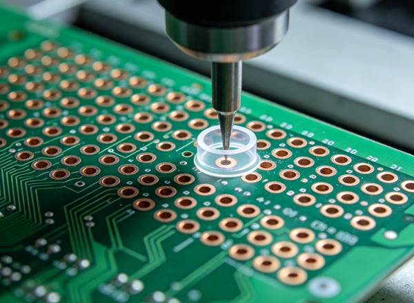
How Drilling Affects PCB Prototype Cost
Drilling requirements can have a noticeable impact on prototypes because engineering and setup costs are distributed across a small number of boards.
A prototype containing:
- Many drill sizes
- Very small holes
- Blind vias
- Microvias
- Back drilling
can require substantially more process planning than a conventional prototype.
This is one reason prototype quotations should include complete fabrication information.
The broader relationship between engineering requirements and prototype pricing is covered in How Much Does PCB Prototyping Cost?.
How Drilling Affects PCB Production Cost
In production, quantity changes the economics.
A complicated drilling structure may become more economical per board when produced at higher volume because setup and engineering costs are distributed across more units.
However, high-volume production also makes process efficiency more important.
For example, thousands of boards with unnecessarily complicated drill structures can create significant cumulative production time.
Therefore, cost optimization should consider both:
Cost per board
and
Total production cost
How to Reduce PCB Drilling Cost
Use the Largest Practical Via Diameter
If the design allows a slightly larger via, it can reduce drilling difficulty.
Do not use an extremely small via simply because the PCB fabricator can manufacture it.
Reduce Unnecessary Drill Sizes
A PCB containing many different hole diameters can require more tool changes.
Standardizing hole sizes where possible can simplify manufacturing.
Avoid Unnecessary Microvias
Microvias are useful when routing density requires them.
If conventional vias can complete the routing, they may provide a simpler manufacturing solution.
Avoid Excessive Via-in-Pad
Use via-in-pad where the component layout actually requires it.
If a conventional BGA fanout can achieve the same result, it may avoid additional filling and planarization requirements.
Review Board Thickness and Hole Size Together
A thick PCB with extremely small holes can create a demanding aspect ratio.
Sometimes changing the hole size slightly can simplify production without changing the board thickness.
Separate PTH and NPTH Requirements
Clearly identify which holes need plating.
This avoids unnecessary processing for mechanical holes.
How to Optimize Drill Sizes Before Fabrication
A practical design review can follow these steps.
Step 1: Export the Drill Table
Review all drill diameters used by the PCB.
Look for unusually small or uncommon sizes.
Step 2: Group Similar Sizes
If two drill sizes are electrically and mechanically interchangeable, consider whether they can be standardized.
Step 3: Identify the Smallest Finished Hole
Check whether the minimum hole is genuinely required.
Step 4: Calculate Aspect Ratio
Compare the smallest hole with the finished PCB thickness.
Step 5: Identify Special Via Structures
Mark:
- Blind vias
- Buried vias
- Microvias
- Stacked vias
- Via-in-pad
- Back-drilled vias
Step 6: Review Manufacturing Alternatives
Ask whether a simpler via structure can achieve the same routing and electrical performance.
Step 7: Compare the Complete PCB Cost
Do not evaluate drilling separately from layer count, stackup, copper weight, and board thickness.
How Drill Requirements Affect PCB Quote Comparison
When comparing PCB quotations, check the drilling specifications line by line.
| Specification | Quote A | Quote B |
|---|---|---|
| Minimum hole | 0.25 mm | 0.20 mm |
| Finished thickness | 1.6 mm | 1.6 mm |
| Via type | Through-hole | Blind + through-hole |
| Microvia | No | Yes |
| Via filling | No | Yes |
| Back drilling | No | Yes |
| Quantity | Same | Same |
These are fundamentally different manufacturing requirements.
A higher quotation may simply reflect the additional fabrication processes.
This is why Why Do PCB Quotes Vary So Much? is best understood through specification-by-specification comparison rather than unit price alone.
PCB Drilling Cost Checklist
Before sending a PCB to fabrication, check:
- Minimum hole diameter is necessary
- Finished hole and drill diameter are clearly defined
- PTH and NPTH are correctly identified
- Hole count has been reviewed
- Drill sizes have been standardized where possible
- Aspect ratio has been checked
- Board thickness has been considered
- Blind vias are necessary
- Buried vias are necessary
- Microvias are necessary
- Via-in-pad is necessary
- Via filling requirements are defined
- Back drilling is required only where justified
- Slots and mechanical cutouts are clearly specified
Frequently Asked Questions
It can. Smaller holes are generally more demanding to drill and plate, especially when combined with a thick PCB or high aspect ratio. The actual cost depends on the manufacturer and complete board structure.
Not necessarily in a simple linear relationship, but a high via count increases drilling and processing time. Very high via density or special via structures can have a greater impact on cost.
Microvias usually involve additional HDI processing and laser drilling, so they can increase fabrication cost compared with conventional through-hole structures.
It can because via-in-pad often requires via filling and additional surface processing. It is commonly used when routing density or BGA layout makes the additional process worthwhile.
In some cases, yes. A slightly larger hole can reduce drilling difficulty and aspect-ratio constraints. However, the hole size must still meet the electrical and mechanical requirements of the design.
Conclusion
PCB drilling cost is determined by much more than the number of holes on the board.
Hole diameter, hole type, aspect ratio, board thickness, via structure, microvias, via filling, back drilling, and drilling tolerances can all affect the manufacturing process.
For standard boards, using practical drill sizes and avoiding unnecessary special structures can help control fabrication cost.
For HDI, high-speed, and high-density designs, however, smaller and more complex via structures may be necessary. In those cases, the goal is not simply to minimize drilling cost, but to find the simplest manufacturing structure that still satisfies the electrical and mechanical requirements.
When reviewing a PCB quotation, TOPFAST can evaluate the drill table together with the stackup, board thickness, copper structure, and via requirements. This gives a more accurate picture of where drilling-related cost is coming from.
Request a PCB Cost Review
Provide the Gerber files and drill files together with the required board thickness, layer count, copper weight, surface finish, and quantity. A complete specification allows the drilling requirements to be evaluated as part of the total PCB fabrication cost.
Optimize the Drill Structure Before Production
Before finalizing the PCB, review the minimum hole size, drill-size distribution, aspect ratio, via types, and special drilling requirements. Small changes made at the design stage are generally easier to implement than process changes after fabrication has started.
 EN
 PT
 AR
 DE
 FR
 ES