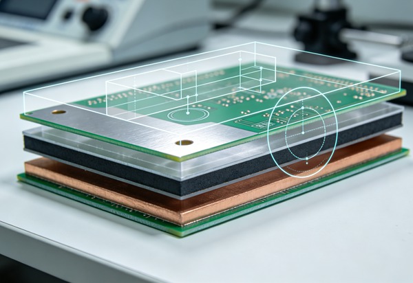
PCB thickness is often treated as a simple mechanical specification, but it can have a direct effect on manufacturing cost.
A standard PCB may use a common thickness such as 1.6 mm, while other applications may require 0.8 mm, 1.0 mm, 1.2 mm, 2.0 mm, or even thicker constructions.
Changing the thickness does not simply mean adding or removing material.
The finished thickness is determined by the combination of:
- Copper layers
- Core materials
- Prepreg
- Copper foil
- Lamination structure
- Surface finish
- Manufacturing tolerances
As a result, an unusual board thickness can affect material selection, stackup design, drilling, lamination, impedance control, mechanical performance, and production yield.
For PCB cost optimization, the important question is not whether a thinner or thicker board is cheaper in isolation.
The practical question is whether the selected thickness is necessary for the product and whether it can be manufactured efficiently.
Table of Contents
What Does PCB Thickness Mean?
PCB thickness normally refers to the finished thickness of the fabricated board.
For a multilayer PCB, this is not simply the thickness of the copper-clad laminate.
The final structure can include:
- Outer copper
- Inner copper
- Core
- Prepreg
- Bonding layers
- Surface finish
For example, a nominal 1.6 mm multilayer PCB may be constructed from several core and prepreg combinations rather than one 1.6 mm sheet.
This is why the specified finished thickness and the actual stackup need to be considered together.
Common PCB Thickness Options
Typical PCB thickness specifications include:
| Finished Thickness | Common Applications |
|---|---|
| 0.4 mm | Compact electronics, small modules |
| 0.6 mm | Thin electronic products |
| 0.8 mm | Compact devices, lightweight designs |
| 1.0 mm | Consumer and industrial electronics |
| 1.2 mm | Compact and general-purpose boards |
| 1.6 mm | Common general-purpose PCB |
| 2.0 mm | Mechanical strength, industrial applications |
| 2.4 mm | Special mechanical requirements |
| 3.0 mm+ | Heavy or specialized PCB structures |
These are not strict application rules.
The appropriate thickness depends on the product’s mechanical, electrical, thermal, and assembly requirements.
Why PCB Thickness Affects Cost
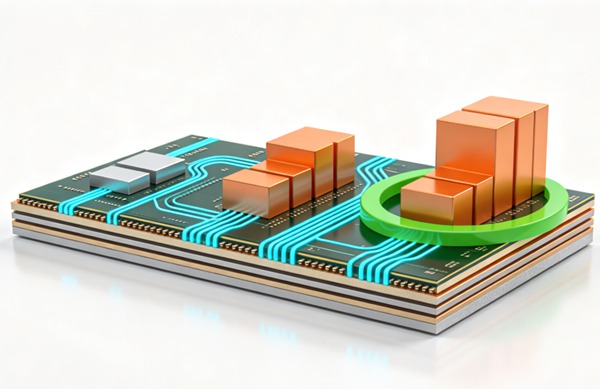
PCB thickness can influence several parts of the manufacturing process.
The main cost factors include:
- Laminate material
- Core thickness
- Prepreg selection
- Copper structure
- Lamination cycle
- Drilling
- Plating
- Mechanical processing
- Impedance control
- Material availability
- Manufacturing yield
A standard thickness may be easier to produce because the required materials and process parameters are commonly available.
An unusual thickness can require a less common stackup or additional engineering work.
Therefore, two boards with exactly the same length and width can have different prices because their finished thicknesses are different.
Is 1.6 mm PCB Always the Cheapest?
Not necessarily.
1.6 mm is widely used and is often a convenient standard for many PCB applications.
However, the lowest-cost option depends on:
- Layer count
- Material
- Copper weight
- Quantity
- Board size
- Stackup
- Surface finish
- Drill requirements
For a two-layer PCB, 1.6 mm may be a straightforward construction.
For a complex multilayer PCB, achieving exactly 1.6 mm may require a particular combination of cores and prepregs.
In some cases, allowing a reasonable thickness tolerance can give the manufacturer more stackup options and potentially improve manufacturing efficiency.
How Thin PCBs Affect Manufacturing Cost
Thin PCBs can reduce material usage, but that does not automatically make them cheaper.
Very thin boards introduce additional manufacturing considerations.
These may include:
- Handling difficulty
- Warpage
- Mechanical deformation
- Drilling stability
- Lamination control
- Assembly handling
- Connector insertion strength
A thin PCB may also require special materials or process controls.
Therefore, reducing the finished thickness from 1.6 mm to 0.8 mm should be based on an actual product requirement.
If the product does not benefit from the thinner construction, the potential material saving may not compensate for the additional manufacturing complexity.
When Is a Thin PCB Worth the Cost?
Thin PCBs can be useful when the product has strict dimensional constraints.
Typical examples include:
- Wearable electronics
- Compact sensors
- Small consumer devices
- Flexible mechanical assemblies
- Space-constrained modules
- Lightweight electronic products
The objective is usually not simply reducing PCB cost.
Instead, thickness reduction can allow the complete product to become:
- Smaller
- Lighter
- Easier to integrate
- More mechanically flexible
In these cases, the PCB may justify a more specialized manufacturing process.
How Thick PCBs Affect Cost
Increasing PCB thickness can also increase manufacturing cost, although the relationship is not linear.
A thicker board may require:
- Additional dielectric material
- Different core selection
- More prepreg
- Special lamination conditions
- Longer drilling
- Modified mechanical processing
For example, a 2.0 mm board is not necessarily 25% more expensive than a 1.6 mm board.
The final price depends on the complete construction.
This is an important point when evaluating PCB quotations.
Thick PCB and Drilling Cost
Board thickness can affect drilling because the drill must pass through a greater amount of material.
This becomes more relevant when the board also contains:
- Small drill diameters
- High aspect-ratio holes
- Large numbers of vias
- Back drilling
- Heavy copper
- Complex multilayer structures
The relationship between thickness and drilling becomes particularly important for high-layer-count boards.
For a more complete evaluation of prototype pricing, see How Much Does PCB Prototyping Cost?.
The same principle applies to production: the drilling specification should be evaluated together with board thickness rather than as an isolated cost item.
PCB Thickness and Aspect Ratio
The relationship between hole diameter and board thickness is important.
A simplified aspect-ratio concept is:
Aspect Ratio = PCB Thickness ÷ Finished Hole Diameter
For example, a 2.0 mm thick board with a 0.2 mm finished hole has a much more demanding aspect ratio than a 1.0 mm board with the same hole diameter.
Higher aspect ratios can increase manufacturing difficulty.
Therefore, if a design uses a thick PCB, the designer should review the smallest holes before finalizing the thickness.
A small increase in hole diameter may sometimes simplify fabrication more effectively than changing the entire board structure.
PCB Thickness and Multilayer Stackup
Thickness becomes increasingly important as layer count increases.
A multilayer PCB needs an appropriate combination of:
- Core
- Prepreg
- Copper foil
- Layer spacing
The finished thickness must be compatible with the required electrical characteristics.
For example, a high-speed multilayer PCB may require specific dielectric thicknesses to achieve the target impedance.
In this situation, forcing the entire stackup to an arbitrary finished thickness can make the design more difficult.
The stackup should instead be developed from the electrical requirements and then checked against the mechanical target.
PCB Thickness and Controlled Impedance
PCB thickness can affect controlled impedance because dielectric geometry is part of the impedance calculation.
For a microstrip or stripline structure, impedance depends on factors including:
- Trace width
- Trace thickness
- Dielectric thickness
- Dielectric constant
- Reference-plane distance
Changing the board thickness does not automatically change impedance, but changing the internal dielectric structure often does.
For high-speed designs, the correct approach is to define the required impedance first and then develop the stackup around that requirement.
Trying to reduce cost by arbitrarily changing board thickness can therefore create additional impedance-design work.
PCB Thickness and Copper Weight Work Together
Board thickness and copper weight should not be evaluated independently.
For example, a PCB may use:
- 1.6 mm finished thickness
- 2 oz outer copper
- 1 oz inner copper
Another design may use:
- 2.0 mm finished thickness
- 1 oz copper throughout
Although the second board is physically thicker, it does not necessarily cost more.
The complete material and manufacturing structure determines the price.
This is why How Copper Weight Affects PCB Cost and Manufacturing should be considered together with board-thickness requirements when optimizing a PCB specification.
PCB Thickness and Surface Finish
Surface finish generally has a smaller direct relationship with board thickness than materials or drilling.
However, the two specifications can appear together in higher-complexity designs.
For example:
- 2.0 mm PCB
- 2 oz copper
- ENIG
- fine-pitch SMT
- controlled impedance
will generally have a different manufacturing cost from:
- 1.6 mm PCB
- 1 oz copper
- HASL
- standard SMT
The final quotation reflects the combined specification.
For this reason, comparing a single cost item without comparing the rest of the PCB construction can lead to an incorrect conclusion.
Does Board Thickness Affect PCB Panelization?
Yes, indirectly.
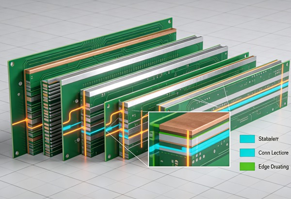
Panelization itself primarily concerns board arrangement, routing, material utilization, tooling rails, and manufacturing efficiency.
However, thicker or thinner PCB constructions can have different mechanical handling requirements.
For example, very thin boards may require additional support during production and assembly.
When evaluating panel utilization, the board’s mechanical characteristics should therefore be considered alongside the number of boards per panel.
See How PCB Panelization Affects PCB Manufacturing Cost for the relationship between panel design and PCB cost.
Standard Thickness vs Custom Thickness
One of the easiest ways to control PCB cost is to determine whether a custom thickness is actually necessary.
A standard thickness may provide:
- More available materials
- More stackup options
- Familiar manufacturing parameters
- Better production efficiency
- Easier quotation comparison
A custom thickness can still be appropriate when the product requires it.
The problem is not using a custom thickness.
The problem is specifying one without a clear engineering reason.
How to Choose PCB Thickness Without Increasing Cost Unnecessarily
Step 1: Determine the Mechanical Requirement
Start with the product enclosure and installation method.
Consider:
- Available space
- Connector position
- Mounting method
- Screw fixing
- Board span
- Mechanical vibration
- Insertion force
If the PCB is mechanically supported by an enclosure, it may not need to be thicker simply for rigidity.
Step 2: Check Electrical Requirements
For multilayer boards, review:
- Impedance
- Dielectric thickness
- Signal integrity
- Crosstalk
- Power distribution
A thinner or thicker board should not be selected before these requirements are understood.
Step 3: Review Component and Assembly Requirements
Consider whether the board must withstand:
- SMT reflow
- Wave soldering
- Through-hole insertion
- Connector insertion
- Mechanical assembly
Very thin PCBs can require additional consideration during assembly handling.
Step 4: Check the Drill Structure
Review:
- Minimum finished hole
- Via diameter
- Aspect ratio
- Through-hole count
- Mechanical holes
A thick board combined with very small holes can increase manufacturing difficulty.
Step 5: Ask for a Manufacturable Stackup
Instead of specifying only:
Finished thickness: 1.6 mm
provide the manufacturer with the complete electrical requirements and let the fabrication team verify the practical stackup.
This is particularly useful for multilayer and high-speed designs.
Step 6: Compare Complete Quotes
When comparing prices, check:
- Finished thickness
- Thickness tolerance
- Layer count
- Copper weight
- Material
- Surface finish
- Drill size
- Quantity
- Testing
- Lead time
A lower price may simply reflect a different PCB construction.
How to Reduce PCB Cost Through Thickness Optimization
Use Standard Thickness When Possible
If the product does not require a special thickness, a commonly available construction can simplify manufacturing.
Do Not Make the PCB Thicker Without a Mechanical Reason
Additional thickness can increase material and processing requirements without necessarily improving electrical performance.
Do Not Make the PCB Thinner Only to Save Material
Very thin boards can introduce mechanical and manufacturing challenges.
The correct thickness is the one that satisfies the complete product requirements.
Allow a Practical Thickness Tolerance
If the mechanical design permits a tolerance rather than an extremely narrow finished-thickness requirement, the manufacturer may have more stackup options.
This can be particularly useful for multilayer PCBs.
Review Thickness Together With Drill Requirements
A thick board with very small holes can be more difficult to fabricate than a thinner board with the same hole size.
If the design permits it, increasing the minimum hole size may sometimes be a more effective cost-control measure than changing the board thickness.
PCB Thickness and Total Manufacturing Cost
PCB thickness should be considered as one part of the complete cost structure:
Material
↓
Layer Count
↓
Copper Weight
↓
Finished Thickness
↓
Drilling
↓
Lamination
↓
Surface Finish
↓
Panelization
↓
Testing
↓
Production Quantity
These factors interact.
For example, increasing layer count can increase the board thickness, but a higher layer count may also allow tighter routing and better signal integrity.
Similarly, reducing thickness may save material but create more difficult drilling or handling conditions.
Therefore, PCB cost optimization should focus on the complete manufacturing structure rather than a single specification.
How to Compare PCB Quotes With Different Board Thicknesses
When two quotations have different prices, first check whether the finished thickness is identical.
For example:
| Specification | Quote A | Quote B |
|---|---|---|
| Layer count | 4L | 4L |
| Finished thickness | 1.0 mm | 1.6 mm |
| Copper | 1 oz | 1 oz |
| Material | FR-4 | FR-4 |
| Surface finish | ENIG | ENIG |
| Quantity | 500 pcs | 500 pcs |
| Board size | Same | Same |
These are not identical PCB specifications.
The difference in price may partly come from the different board construction.
This is why a proper quotation comparison should normalize the technical specifications before evaluating the price difference.
For a broader approach, see Why Do PCB Quotes Vary So Much?.
PCB Thickness Cost Checklist
Before releasing a PCB for quotation, check:
- Finished board thickness is specified
- Thickness tolerance is defined
- Mechanical requirements have been reviewed
- Stackup requirements are understood
- Controlled impedance requirements are considered
- Copper weight is specified
- Minimum hole size is checked
- Hole aspect ratio is acceptable
- Assembly handling requirements are considered
- Standard thickness has been considered
- Custom thickness has a clear engineering reason
- All quotations use the same thickness specification
Frequently Asked Questions
It can be, but not necessarily by a fixed percentage. Material selection, stackup, layer count, copper weight, drilling, quantity, and manufacturing requirements all affect the final price.
1.6 mm is a widely used standard thickness and can be economical for many applications. However, the actual cost depends on the complete PCB construction and production quantity.
No. Very thin boards can require additional handling, lamination, drilling, or assembly controls. A thinner board may therefore have a higher manufacturing cost in some applications.
Yes. The dielectric geometry used in the stackup is an important part of impedance design. Changing the thickness structure can therefore require impedance recalculation.
There is no universal thickness for all multilayer boards. The selection should consider mechanical requirements, stackup, impedance, copper weight, drilling, assembly, and the product enclosure.
Conclusion
PCB thickness is more than a mechanical dimension. It affects the material structure, stackup, drilling, lamination, impedance, handling, and ultimately the manufacturing cost.
A standard thickness can often simplify production, but there are many situations where a thinner or thicker board is technically justified.
The most effective cost strategy is therefore not to select the thinnest or thickest board. Instead, determine the mechanical and electrical requirements first, then select a practical thickness and stackup that can be manufactured consistently.
For complex multilayer and high-speed PCB projects, TOPFAST can review finished thickness together with the stackup, copper structure, drill requirements, and impedance targets before production. This helps avoid a situation where a nominal thickness requirement creates unnecessary manufacturing cost.
Request a PCB Cost Review
When requesting a quotation, provide the finished thickness, thickness tolerance, layer count, copper weight, material, minimum drill, surface finish, and quantity. This gives the manufacturer enough information to evaluate the actual fabrication cost.
Compare PCB Prices on Equivalent Specifications
If two PCB quotations have different prices, check the board thickness and stackup before comparing the unit prices. A difference in finished thickness can represent a difference in the underlying manufacturing construction.
 EN
 PT
 AR
 DE
 FR
 ES