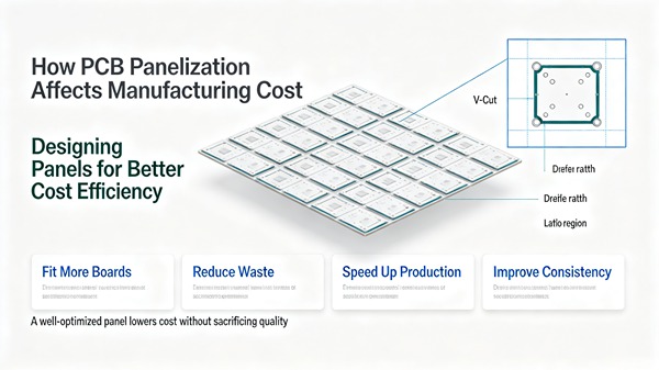
The price of an individual PCB is not determined only by the board itself.
The way multiple boards are arranged on a manufacturing panel can also affect the final cost.
This process is known as PCB panelization.
Instead of manufacturing every PCB as a completely separate piece, manufacturers normally arrange multiple boards on a larger production panel.
The panel can then go through fabrication and, when required, assembly as a combined unit.
The number of usable PCBs that can be obtained from one panel affects:
- Material utilization
- Production efficiency
- Tooling
- Routing time
- Handling
- Assembly throughput
- Effective cost per board
For high-volume production, even a small improvement in panel utilization can have a noticeable effect on total manufacturing cost.
Table of Contents
What Is PCB Panelization?
PCB panelization means arranging multiple individual PCB designs onto a larger manufacturing panel.
A simplified example is:
Individual PCB → panel arrangement → fabrication → separation
The panel may contain:
- Repeated copies of one PCB
- Multiple PCB variants
- Tooling rails
- Fiducials
- Breakaway tabs
- V-grooves
- Routing paths
The exact arrangement depends on the PCB dimensions, shape, manufacturing process, and assembly requirements.
Why Panelization Affects PCB Cost
Imagine two panel layouts.
Layout A
8 boards per panel
Layout B
10 boards per panel
If the manufacturing cost of the panel remains approximately similar, Layout B distributes that cost across more usable boards.
This can reduce the effective manufacturing cost per PCB.
However, panelization is not simply a matter of fitting as many boards as possible onto a sheet.
The panel still needs enough space for:
- Routing
- V-grooves
- Tooling
- Handling
- Electrical clearance
- Assembly equipment
An aggressive layout that creates manufacturing problems may cost more overall.
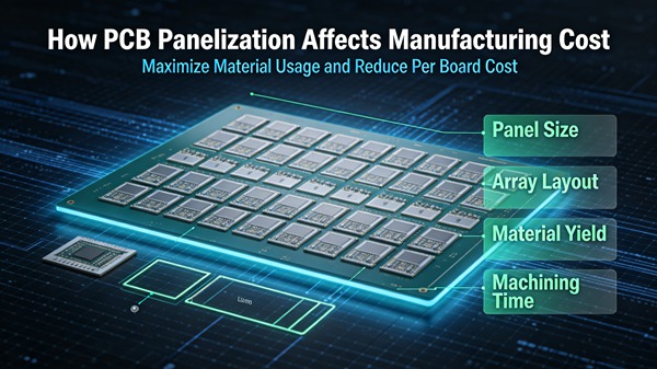
Board Size Is One of the First Variables
The dimensions of the PCB directly affect how many units can fit on a panel.
For example:
50 × 50 mm
and
100 × 100 mm
boards require very different panel arrangements.
But the relationship is not always linear.
A small change in board dimensions can sometimes allow a much better arrangement.
For example, changing one dimension slightly may allow:
- More boards per row
- Better rotation
- Less unused material
This is why board outline should be considered together with panelization when the mechanical design still has some flexibility.
Board Shape Also Matters
A rectangular PCB is usually easier to panelize than an irregular shape.
Common cost challenges include:
- Large cutouts
- Rounded sections
- Narrow extensions
- Multiple slots
- Complex internal routing
These features may increase material waste or require more routing.
If the mechanical design permits it, simplifying the board outline can improve manufacturing efficiency.
V-Groove vs Routing
Two common PCB separation methods are:
V-Groove
A groove is cut along straight lines so the boards can later be separated.
V-groove works well for boards with:
- Straight edges
- Regular shapes
- Repeated rectangular outlines
Routing
A router cuts around the PCB outline.
Routing is more suitable for:
- Irregular shapes
- Curved outlines
- Internal cutouts
However, routing consumes additional panel space and requires tool movement around the board.
The appropriate method depends on the board geometry.
When V-Groove Is More Efficient
If several identical rectangular boards can be placed next to each other with straight boundaries, V-groove may allow efficient panel utilization.
For example:
Board | Board | Board | Board
can often be processed efficiently.
But V-groove is not suitable for every design.
The final PCB must still meet the required edge conditions after separation.
When Routing Is Necessary
Routing is often required when the PCB has:
- Curved edges
- Irregular shapes
- Internal slots
- Complex cutouts
In these cases, trying to force a V-groove arrangement may create mechanical problems.
The slightly higher fabrication cost can be justified if the board shape itself is necessary.
Tooling Rails Take Up Space
Production panels often require rails around the board area.
These rails may be used for:
- Machine handling
- Conveyor transport
- Fiducials
- Assembly alignment
- Tooling holes
The available area for actual PCBs is therefore smaller than the total panel dimensions.
This is especially important for SMT assembly.
A panel designed only for PCB fabrication may not be ideal for automated assembly.
Panelization for PCB Fabrication vs SMT Assembly
There is an important difference between fabrication panelization and assembly panelization.
A PCB fabrication panel focuses primarily on:
- Material utilization
- Drilling
- Imaging
- Routing
- Electrical testing
An SMT assembly panel also needs to consider:
- Pick-and-place access
- Solder paste printing
- Fiducials
- Conveyor handling
- Component clearance
- Depanelization
A layout that looks efficient for PCB fabrication may not necessarily be the best choice for SMT.
For assembled products, both stages should be considered together.
Panelization Can Affect Assembly Yield
Panelization is not only a cost issue.
A poor panel design can also create assembly problems.
For example:
- Excessive board flexing
- Uneven support
- Insufficient tooling
- Poor fiducial placement
- Component clearance problems
These can affect:
- Solder paste printing
- Component placement
- Reflow
- Inspection
Therefore, the cheapest theoretical panel is not always the best production panel.
How-To: Optimize PCB Panelization
Step 1: Start With the Finished PCB
First define:
- Board dimensions
- Board outline
- Component locations
- Connector positions
- Mechanical requirements
Do not modify the PCB outline solely to improve panel utilization if the change creates a product-level problem.
Step 2: Test Different Orientations
A PCB does not always need to be placed in the same orientation.
Try:
- 0°
- 90°
- 180°
- Mirrored arrangements where manufacturing permits
Different orientations can sometimes produce substantially different material utilization.
Step 3: Calculate Boards Per Panel
Compare several realistic layouts.
For example:
| Layout | Boards/Panel | Relative Utilization |
|---|---|---|
| A | 6 | Lower |
| B | 8 | Moderate |
| C | 10 | Higher |
The exact result depends on panel dimensions and manufacturing constraints.
Step 4: Check Separation Requirements
Determine whether the design can use:
- V-groove
- Tab routing
- Perforated tabs
- Full routing
Do not optimize material utilization before checking whether the boards can actually be separated safely.
Step 5: Add Assembly Requirements
If the boards will be assembled, check:
- Tooling rails
- Fiducials
- Solder paste printing
- Component clearance
- Conveyor requirements
The panel must work for the complete production process.
Step 6: Compare the Effective Cost
A useful metric is:
Effective PCB cost = panel cost ÷ usable PCB quantity
This is more useful than simply looking at the panel price.
For example:
$100 panel ÷ 10 boards = $10 per board
while:
$100 panel ÷ 6 boards = $16.67 per board
The actual quotation may contain additional costs, but this calculation illustrates why utilization matters.
Panelization and PCB Quantity
Quantity can influence the ideal panel configuration.
Suppose the customer needs:
100 boards
If the panel contains:
10 boards
then the production quantity aligns neatly with:
10 panels
If the panel contains:
7 boards
the manufacturer may need to produce a different number of panels and manage additional unused pieces.
This does not always create a major cost difference, but production quantity and panel quantity should be considered together.
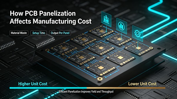
Mixed PCB Panelization
Some projects contain several related PCB designs.
For example:
- Main board
- Control board
- Display board
- Sensor board
In certain circumstances, multiple designs can be placed on one production panel.
This may improve material utilization.
However, mixed panelization introduces additional considerations:
- Different quantities
- Different fabrication requirements
- Different test requirements
- Depanelization
- Assembly configuration
It should therefore be evaluated on a project-by-project basis.
Panelization and Small PCB Designs
Small PCBs can sometimes benefit significantly from panelization.
A single tiny PCB may occupy only a small portion of the manufacturing panel.
Placing many copies together improves material utilization and production handling.
This is particularly useful for:
- Sensor boards
- Wearable electronics
- Small controllers
- RF modules
- IoT boards
However, small boards also need sufficient support during SMT assembly.
Panelization and Large PCBs
Large PCBs create a different challenge.
The board may occupy most of the available panel area.
There may be limited opportunities to increase the number of boards per panel.
In this case, cost optimization may come from:
- Board outline optimization
- Material selection
- Panel size selection
- Manufacturing yield
- Reducing unnecessary cutouts
rather than simply increasing board count per panel.
Should You Design the PCB Around Panelization?
Not entirely.
The product’s electrical and mechanical requirements should come first.
But panelization should be considered before the design is completely frozen.
If the board outline can be changed by a few millimeters without affecting the product, that flexibility may be valuable.
A manufacturing engineer can then compare several arrangements before the final mechanical design is locked.
Common Panelization Mistakes
Designing Only One Board at a Time
The individual PCB may be manufacturable but inefficient on the panel.
Ignoring SMT Requirements
A fabrication-friendly panel may not work well with the assembly line.
Using Too Many Internal Cutouts
Cutouts can reduce material utilization and increase routing operations.
Ignoring Depanelization
Components placed too close to the board edge can be damaged during separation.
Optimizing for Maximum Board Count Only
The maximum number of boards is not always the best layout if it creates assembly or reliability problems.
How-To: Reduce PCB Cost Through Panelization
A practical review can follow this sequence:
Board outline
↓
Panel size
↓
Board orientation
↓
V-groove or routing
↓
Tooling rails
↓
Fiducials
↓
Assembly clearance
↓
Depanelization
↓
Boards per panel
↓
Effective cost per PCB
This approach is more reliable than simply asking for the smallest possible panel price.
Does Panelization Affect PCB Quality?
It can.
Poor panelization can increase:
- Board warpage
- Mechanical stress
- Depanelization damage
- Assembly problems
- Handling issues
For example, an extremely long and narrow panel may have different mechanical behavior from a balanced panel.
The manufacturing panel therefore needs to satisfy both cost and process requirements.
FAQ
It can. Better panel utilization allows the cost of the manufacturing panel to be distributed across more usable PCBs.
There is no universal number. The optimum quantity depends on board dimensions, panel size, routing requirements, tooling, assembly equipment, and production quantity.
It can be more efficient for suitable rectangular boards, but routing is necessary for many irregular shapes. The correct choice depends on the PCB outline and production process.
Yes. Assembly panels must consider fiducials, tooling rails, conveyor handling, solder paste printing, component clearance, and depanelization.
If the mechanical design allows some flexibility, it can be worthwhile. But electrical, mechanical, and reliability requirements should remain the priority.
Conclusion
PCB panelization is easy to overlook because it happens after the PCB design appears to be complete.
In reality, it can influence the effective manufacturing cost of every board produced.
The most important factors include:
- Board size
- Board shape
- Panel dimensions
- Board orientation
- V-groove
- Routing
- Tooling rails
- Assembly requirements
- Depanelization
- Production quantity
The best panel is not necessarily the one containing the maximum number of boards.
It is the panel that provides a good balance between material utilization, manufacturing efficiency, assembly stability, and product quality.
For production projects, reviewing panelization before the PCB design is fully frozen can prevent unnecessary material waste and make the transition from prototype to volume manufacturing smoother.
TOPFAST can evaluate panel utilization together with the fabrication and assembly requirements, which is particularly useful when a board is moving from engineering builds into recurring production.
 EN
EN  PT
PT  AR
AR  DE
DE  FR
FR  ES
ES