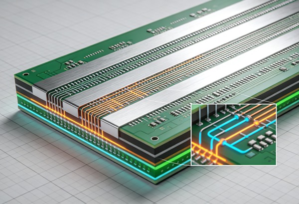
Copper weight is one of the PCB specifications that can noticeably change manufacturing cost, especially when a design moves from standard 1 oz copper to 2 oz, 3 oz, or heavier copper.
The effect is not simply the price of additional copper. Heavier copper can also change etching requirements, plating time, trace geometry, minimum spacing, thermal behavior, drilling conditions, and the manufacturing process itself.
For a simple low-current control board, increasing copper thickness without a clear electrical or thermal reason can add unnecessary cost. For power electronics, automotive power systems, battery applications, and high-current circuits, however, heavier copper may be required to meet the electrical and thermal requirements.
Understanding this relationship helps engineers specify the copper weight based on the actual design requirements rather than selecting a heavier specification by default.
Table of Contents
What Does PCB Copper Weight Mean?
PCB copper weight describes the amount of copper contained in a defined surface area of copper foil.
In PCB manufacturing, the commonly used unit is oz/ft², or ounces per square foot.
Typical copper weights include:
- 0.5 oz
- 1 oz
- 1.5 oz
- 2 oz
- 3 oz
- 4 oz
- 6 oz
- 8 oz and above for heavy copper applications
For standard PCB production, 1 oz copper is one of the most common specifications.
The nominal copper thickness associated with common copper weights is approximately:
| Copper Weight | Approx. Copper Thickness |
|---|---|
| 0.5 oz | 17 µm |
| 1 oz | 35 µm |
| 1.5 oz | 52 µm |
| 2 oz | 70 µm |
| 3 oz | 105 µm |
| 4 oz | 140 µm |
| 6 oz | 210 µm |
Actual finished copper thickness can differ from the nominal foil thickness because PCB fabrication may add copper during plating.
This distinction becomes particularly important for plated-through holes and outer-layer copper.
Why Does Copper Weight Affect PCB Cost?
Copper weight influences PCB cost through several different mechanisms.
The most obvious factor is the additional copper material itself. However, material cost is only one part of the equation.
Higher copper weight can also increase:
- Copper material consumption
- Lamination requirements
- Plating time
- Etching difficulty
- Chemical consumption
- Production cycle time
- Process control requirements
- Finished-board weight
- Manufacturing complexity
As copper becomes thicker, maintaining the required trace geometry can also become more difficult.
This means a 2 oz PCB is not simply a 1 oz PCB with twice as much copper.
The production process may need to be adjusted to accommodate the thicker copper.
1 oz Copper: The Standard Cost Baseline
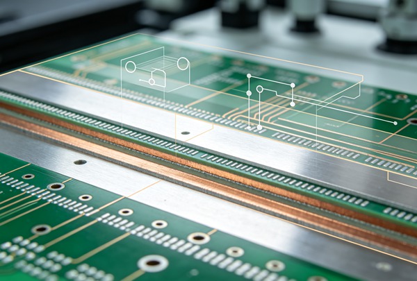
For many digital, control, communication, and general-purpose electronic boards, 1 oz copper provides a practical balance between electrical performance and manufacturing cost.
It is commonly suitable when:
- Current requirements are moderate
- Standard trace widths can be used
- Thermal loads are manageable
- The design does not require heavy copper
- Standard fabrication rules are acceptable
If the design can meet its electrical requirements using 1 oz copper, there is usually little reason to specify 2 oz simply as a safety margin.
The actual requirement should instead be determined from trace current, temperature rise, available routing area, voltage drop, and thermal design.
For cost-sensitive products produced in larger quantities, avoiding unnecessary copper weight can have a meaningful effect on the total PCB cost.
How 2 oz Copper Changes PCB Pricing
Moving from 1 oz to 2 oz copper introduces both material and process considerations.
The additional copper increases material usage, but the more important issue can be manufacturing complexity.
With 2 oz copper, designers may need to consider:
- Larger minimum spacing
- Wider traces
- Different etching compensation
- Increased copper distribution requirements
- Higher plating requirements
- Thermal expansion behavior
- Larger pads or current-carrying structures
For many power-related boards, 2 oz copper is still a relatively practical specification.
The key question is not whether 2 oz is more expensive than 1 oz. It is.
The useful question is whether the additional copper solves an actual electrical or thermal requirement.
When Heavy Copper Has a Larger Cost Impact
Heavy copper generally refers to PCB structures using substantially thicker copper than standard boards.
Depending on the manufacturer and application, heavy copper may involve 3 oz, 4 oz, 6 oz, 8 oz, or even thicker copper.
Heavy copper is often used for:
- Power supplies
- Battery management systems
- Motor controllers
- EV power electronics
- Industrial power equipment
- High-current distribution
- Inverters
- Automotive power circuits
- High-current connectors
The cost impact can become more significant because several manufacturing processes need to accommodate the increased copper thickness.
For example, thick copper can make fine-line etching more difficult. At the same time, the designer may need wider traces and larger clearances.
This can affect the overall board layout rather than just the material specification.
Copper Weight and Trace Width Are Closely Related
One of the most important cost considerations is the relationship between copper thickness and trace width.
A higher copper weight allows more current to flow through a conductor, but current capacity is not determined by copper weight alone.
Trace width and allowable temperature rise also matter.
For example, instead of immediately changing a design from 1 oz to 2 oz copper, an engineer may be able to increase the width of a high-current trace.
This can sometimes provide the required current capacity without changing the copper specification across the entire board.
However, this approach depends on available routing space.
If the board is densely routed, increasing trace width may not be practical.
In that situation, increasing copper thickness may be a more appropriate solution.
Does More Copper Always Mean Better PCB Performance?
No.
Higher copper weight can improve current-carrying capability and help manage heat, but it also introduces design and manufacturing trade-offs.
A heavier copper specification can create problems when combined with very fine features.
For example, a board requiring both:
- very thick copper, and
- very fine traces and spacing
can become considerably more difficult to manufacture.
The designer therefore needs to balance:
Current capacity + thermal performance + routing density + manufacturing capability + cost
rather than treating copper thickness as an independent specification.
Copper Weight and PCB Layer Design
Copper weight can be specified differently for different layers.
For example, a multilayer PCB might use:
- 1 oz inner layers
- 1 oz standard signal layers
- 2 oz outer power layers
This can be more economical than specifying 2 oz copper throughout the entire board.
The correct approach depends on the current distribution and thermal requirements of the design.
For a power PCB, the outer layers may carry high-current paths while internal signal layers handle low-current functions.
Using different copper weights where appropriate can therefore reduce unnecessary material and processing costs.
For multilayer boards, copper distribution also needs to be considered during stackup development.
Designers working with complex layer structures should evaluate copper balance before manufacturing rather than changing copper weight after the layout is complete.
How Copper Weight Affects PCB Panelization Cost
Copper weight and panel utilization can interact in ways that are easy to overlook.
If a panel contains a large amount of copper, the material value of the panel increases.
At the same time, the manufacturing process must maintain relatively consistent copper distribution.
Large differences between copper-heavy areas and copper-light areas can influence plating and etching behavior.
Panelization therefore needs to consider more than simply fitting as many boards as possible onto one panel.
The relationship between panel utilization and manufacturing cost is discussed in more detail in PCB Manufacturing Cost.
For high-copper designs, panel layout should be reviewed together with copper distribution rather than treated as a separate step.
Copper Weight and PCB Prototype Cost
Copper weight can also affect prototype pricing.
A prototype using 2 oz or 3 oz copper may require different process conditions from a standard 1 oz prototype.
This becomes more relevant when the prototype includes:
- Heavy copper
- Large current paths
- High-current vias
- Large copper areas
- Tight spacing
- Controlled impedance
- Mixed copper weights
When comparing prototype quotations, the copper specification should be included in the RFQ rather than simply requesting a generic PCB price.
For a broader explanation of prototype pricing, see How Much Does PCB Prototyping Cost?.
Copper Weight and Surface Finish
Copper thickness and surface finish are separate specifications, but they can influence the final manufacturing price together.
For example, a board may require:
- 2 oz copper
- ENIG
- controlled impedance
- small vias
- tight tolerances
The final cost reflects the combination of these requirements rather than the copper weight alone.
This is one reason two boards with identical dimensions can receive substantially different quotations.
When comparing quotations, the complete specification should be reviewed rather than comparing only the price per board.
This is also why PCB quote comparison should focus on specification equivalence before comparing unit prices.
Does Heavy Copper Increase PCB Material Cost?
Yes, but material cost is only one component.
A simplified cost structure can be viewed as:
PCB Cost = Material + Processing + Tooling + Testing + Setup + Logistics + Manufacturing Margin
Increasing copper weight primarily affects the material and processing portions.
The actual percentage increase varies depending on:
- Board size
- Layer count
- Copper distribution
- Copper weight on each layer
- Quantity
- Material type
- Surface finish
- Drill structure
- Production process
- Required tolerances
Therefore, there is no universal rule such as “2 oz copper costs exactly twice as much as 1 oz copper.”
How to Choose Copper Weight Without Overpaying
The most effective way to control copper-related cost is to start from electrical requirements.
Step 1: Identify the highest-current circuits
List the power rails and high-current paths on the board.
Separate them from low-current signal traces.
For example:
- Digital signals
- Sensor circuits
- Communication lines
- Control signals
usually have very different requirements from:
- Motor power
- Battery connections
- DC/DC converter outputs
- High-current switching paths
Step 2: Calculate the required trace width
Determine the required conductor width based on:
- Current
- Copper thickness
- Allowable temperature rise
- Trace length
- Thermal environment
Do not increase copper weight automatically before checking whether wider traces can solve the problem.
Step 3: Check available routing space
If the calculated trace width fits comfortably within the available PCB area, standard copper may be sufficient.
If it does not, increasing copper thickness may reduce the required trace width for a given current requirement.
However, the actual design should be verified against the applicable engineering standard and manufacturing capability.
Step 4: Consider copper by layer
Ask whether the entire PCB actually needs heavier copper.
If only a few layers carry high current, a mixed copper structure may be more economical than using heavy copper across all layers.
Step 5: Check manufacturability
Before finalizing the specification, review:
- Minimum trace width
- Minimum spacing
- Via structure
- Finished copper thickness
- Plating requirements
- Board thickness
- Layer stackup
- Copper distribution
A design that is electrically correct but difficult to fabricate may increase cost more than expected.
Step 6: Request a specification-based quotation
The RFQ should clearly identify copper requirements.
For example:
4-layer PCB, 1 oz inner copper, 2 oz outer copper, FR-4, ENIG, 1.6 mm finished thickness.
This is much more useful than simply requesting:
4-layer PCB quotation.
The more complete the specification, the easier it is to compare quotations on an equivalent basis.
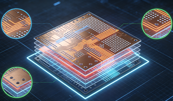
How to Reduce PCB Cost When Heavy Copper Is Required
Heavy copper should not necessarily be removed simply to reduce cost.
Instead, look for ways to limit where it is required.
Use Heavy Copper Only Where Necessary
If only the power layers need additional copper, consider using heavier copper selectively.
This can avoid increasing copper weight across the entire stackup.
Increase Trace Width Where Space Allows
If the PCB has enough routing space, wider traces may provide the required current capacity without increasing copper thickness.
This is especially useful for relatively simple power-routing areas.
Optimize Board Size
A larger board with heavy copper can increase material consumption significantly.
Reducing unused board area can therefore reduce both base material and copper-related cost.
Review Panel Utilization
Efficient panelization can reduce material waste.
However, the panel should still maintain suitable copper distribution and fabrication stability.
Avoid Unnecessary Heavy Copper on Signal Layers
Signal layers rarely need the same copper thickness as high-current power layers.
Using a uniform heavy-copper specification without a design requirement can increase cost and complicate fine-pitch routing.
How to Compare Two PCB Quotes With Different Copper Weights
Suppose two suppliers provide quotations for the same board.
One quotation specifies:
- 1 oz copper
- Standard fabrication
The other specifies:
- 2 oz copper
- Different fabrication conditions
The second quote should not automatically be considered expensive simply because its unit price is higher.
First confirm whether the specifications are actually equivalent.
Compare:
| Specification | Quote A | Quote B |
|---|---|---|
| Layer count | Same? | Same? |
| Copper weight | 1 oz | 2 oz |
| Board thickness | Same? | Same? |
| Material | Same? | Same? |
| Surface finish | Same? | Same? |
| Trace/space | Same? | Same? |
| Via structure | Same? | Same? |
| Quantity | Same? | Same? |
| Testing | Same? | Same? |
| Lead time | Same? | Same? |
If the copper weight differs, the quotations are not directly comparable until that difference is accounted for.
How Copper Weight Fits Into Total PCB Cost
Copper is only one part of PCB pricing.
A practical cost model should consider:
Board Size
↓
Layer Count
↓
Material
↓
Copper Weight
↓
Drilling / Via Structure
↓
Surface Finish
↓
Panelization
↓
Testing and Tooling
↓
Quantity and Production Volume
These factors interact.
For example, increasing copper weight may also affect the trace geometry, panel design, plating requirements, and production process.
That is why PCB cost should be evaluated as a complete manufacturing specification rather than as a collection of isolated price items.
For a broader overview of the factors affecting PCB quotations, see Why Do PCB Quotes Vary So Much?.
When Should You Specify 2 oz Copper?
2 oz copper can be considered when the design has a clear requirement for:
- Higher current capacity
- Lower conductor resistance
- Improved thermal conduction
- Wider thermal margins
- Power distribution
- High-current switching
- Battery or motor power paths
It should not be selected solely because “more copper is better.”
If a standard 1 oz design already satisfies the electrical and thermal requirements, moving to 2 oz may provide little practical benefit while increasing manufacturing cost.
When Is Heavy Copper Worth the Additional Cost?
For some power applications, heavy copper is part of the functional design rather than an optional upgrade.
Examples include boards carrying substantial current through relatively limited PCB area.
In these applications, the additional manufacturing cost may be justified by the electrical requirements.
The engineering decision should therefore consider the complete product design:
- Current
- Voltage
- Temperature
- Available board area
- Cooling method
- Reliability requirements
- Expected operating conditions
- Manufacturing capability
The objective is not to minimize copper weight at all costs. The objective is to use enough copper to meet the actual design requirement without unnecessarily increasing the manufacturing specification.
Practical PCB Copper Weight Cost Checklist
Before releasing a PCB for quotation, check the following:
- Copper weight is specified for each relevant layer
- High-current traces have been identified
- Trace width has been calculated
- Temperature rise requirement has been considered
- Heavy copper is used only where necessary
- Via current capacity has been reviewed
- Copper distribution is reasonably balanced
- Panelization has been considered
- Board thickness is compatible with the copper structure
- Manufacturing capability has been confirmed
- The RFQ includes complete copper specifications
This checklist can prevent a common costing problem: specifying a more expensive copper structure before determining whether the design actually needs it.
Frequently Asked Questions
Yes. The additional copper material and manufacturing processing generally increase the PCB cost. The actual difference depends on board size, layer count, quantity, copper distribution, and other specifications.
For many standard electronic and control boards, 1 oz copper is a common starting point. Whether it is sufficient depends on current, temperature rise, trace width, thermal conditions, and the specific circuit design.
Higher copper thickness can increase current-carrying capability, but it does not mean traces can always be made proportionally narrower. Etching and manufacturing constraints still apply, and the actual geometry needs to be designed and verified accordingly.
Yes. A multilayer PCB can use different copper weights on different layers when the stackup and manufacturing process support it. This can be useful when only specific layers carry high current.
Not automatically. Heavy copper can provide electrical and thermal advantages, but overall reliability also depends on materials, lamination, thermal cycling, plating, vias, soldering, mechanical design, and operating conditions.
Conclusion
Copper weight is a direct PCB cost factor, but its effect goes beyond the price of copper itself.
Moving from 1 oz to 2 oz or heavier copper can change the fabrication process, trace geometry, plating requirements, panel design, and manufacturing conditions. For high-current applications, these additional requirements may be necessary. For standard signal and control boards, however, heavier copper may add cost without providing a meaningful design benefit.
The most practical approach is to determine the required current capacity and thermal performance first, then select the copper structure that satisfies those requirements.
For PCB manufacturers such as TOPFAST, a complete RFQ that specifies copper weight by layer, board thickness, layer count, trace requirements, and other critical parameters makes it much easier to evaluate the actual manufacturing cost rather than relying on a generic board price.
Request a PCB Cost Review
If your design uses 2 oz, 3 oz, or heavier copper, you can submit the complete PCB specification for a quotation and manufacturing review. The copper structure can then be evaluated together with the stackup, routing density, and production requirements.
Review the Complete PCB Cost
Copper weight is only one component of PCB pricing. For a complete cost evaluation, compare it together with material, panelization, tooling, quantity, surface finish, and fabrication requirements.
 EN
EN  PT
PT  AR
AR  DE
DE  FR
FR  ES
ES