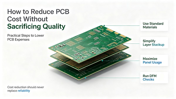
Reducing PCB cost is often treated as a purchasing exercise.
In practice, some of the largest savings are determined before a quotation is even requested.
The PCB design itself controls many of the factors that affect manufacturing cost:
- Layer count
- Board dimensions
- Material
- Copper weight
- Drill structure
- Trace width and spacing
- Surface finish
- Tolerances
- Testing requirements
- Production quantity
A cheaper material or lower quotation may reduce the initial purchase price, but it can also create problems during assembly or field operation.
A better approach is to remove unnecessary manufacturing complexity while keeping the requirements that actually affect product performance.
Table of Contents
Start With the PCB Requirements, Not the Price
Before trying to reduce cost, separate the requirements into three categories.
Requirements That Cannot Be Compromised
These may include:
- Current capacity
- Operating temperature
- Required impedance
- Mechanical dimensions
- Safety requirements
- Reliability targets
These should remain unchanged unless the product specification itself changes.
Requirements That Can Be Optimized
Examples include:
- Layer count
- Stackup
- Board outline
- Via structure
- Copper distribution
- Surface finish
These are often where meaningful savings can be found.
Requirements That May Be Unnecessary
Examples include:
- Extremely tight tolerances without a functional reason
- Special materials used by default
- HDI features that are not required
- Excessive copper weight
- Over-specified surface finishes
This classification makes cost reduction much more systematic.
1. Optimize Layer Count
Layer count is one of the first things to review.
A 6 layer PCB does not automatically provide better value than a 4 layer PCB.
Likewise, reducing an 8 layer design to 6 layers is not necessarily a saving if it causes:
- More difficult routing
- More vias
- Signal integrity problems
- Larger board dimensions
- Additional design iterations
The objective is to find the lowest practical layer count that meets the complete electrical and mechanical requirements.
For example, a 4 layer design may be ideal for a controller, while an 8 layer structure may be more appropriate for a dense high-speed board.
2. Review the Stackup Before Routing
Stackup decisions made late in the design can create unnecessary cost.
The stackup affects:
- Impedance
- Signal return paths
- Power distribution
- Dielectric thickness
- Material selection
- Copper distribution
For high-speed designs, stackup should be established before detailed routing begins.
A well-planned stackup can sometimes eliminate the need for more expensive structures later.
For the engineering side of this decision, see PCB Stackup Design.
3. Use the Right Material, Not the Cheapest Material
Standard FR-4 is often sufficient.
However, some applications genuinely require:
- High-Tg materials
- Low-loss laminates
- High-frequency materials
- Low-CTE materials
The wrong approach is to choose a low-cost laminate without checking its suitability.
The other extreme is also common: specifying an expensive material simply because the product is considered “high performance.”
Material selection should be based on:
- Operating temperature
- Frequency
- Signal loss
- Mechanical requirements
- Reliability requirements
If standard FR-4 meets the actual specification, there may be little benefit in paying for a more specialized material.
4. Reduce Unnecessary HDI Features
HDI can solve difficult routing problems, but it should not be used automatically.
Review whether the design really needs:
- Microvias
- Stacked microvias
- Blind vias
- Buried vias
- Via-in-pad
- Sequential lamination
A conventional through-hole structure is generally simpler to manufacture.
If a board can be routed successfully without HDI, there may be little reason to introduce additional fabrication steps.
On the other hand, if a fine-pitch BGA or compact mechanical envelope genuinely requires HDI, removing it may simply move the problem somewhere else.
The trade-off is discussed in more detail in HDI PCB Cost.
5. Review the Board Outline
Board size directly affects material consumption, but the shape of the PCB also matters.
A board with an unusual outline may produce more material waste during panelization.
When the mechanical design allows some flexibility, consider:
- Straight edges
- Fewer cutouts
- More efficient dimensions
- Better panel utilization
Even a small change can sometimes improve the number of boards that fit onto a production panel.
This becomes more significant as production volume increases.
6. Improve Panel Utilization
Panelization is one of the easiest areas to overlook.
Imagine a production panel that accommodates:
8 boards
An optimized arrangement might fit:
10 boards
The individual PCB has not changed electrically, but the amount of usable material per board has improved.
Panel utilization depends on:
- Board dimensions
- Board shape
- Rotation
- Tooling rails
- V-groove
- Routing
- Spacing requirements
For production projects, panelization should therefore be considered before finalizing the mechanical outline.
7. Avoid Unnecessarily Heavy Copper
Heavy copper is useful when the design needs it.
Typical reasons include:
- High current
- Power distribution
- Thermal management
- Reduced conductor resistance
But applying heavy copper to every layer can add unnecessary material and process cost.
For a mixed-signal board, it may be more appropriate to use heavier copper only where the power design requires it, provided the fabrication process and stackup support that construction.
8. Use Practical Trace Width and Spacing
Extremely fine geometry can increase manufacturing difficulty.
If the design uses:
- Very narrow traces
- Very small spacing
- Small annular rings
without a strong electrical reason, there may be an opportunity to simplify the fabrication requirements.
This can have two benefits:
- Lower manufacturing complexity
- Better production robustness
The goal is not to use the largest possible traces.
It is to avoid designing unnecessarily close to the manufacturing limit.
9. Reconsider Tight Tolerances
Tight tolerances are useful when they control an actual product requirement.
But not every dimension needs the same tolerance.
For example, a mechanical interface may require a tight dimensional tolerance while an internal feature has much more flexibility.
Applying an unnecessarily tight tolerance across the entire PCB can increase production difficulty.
A better approach is to identify which dimensions actually matter.
10. Choose the Surface Finish for the Application
Surface finish should be selected based on assembly and reliability requirements.
Common options include:
- HASL
- Lead-free HASL
- ENIG
- OSP
- Immersion silver
For a conventional board, a less expensive finish may be completely adequate.
For fine-pitch components, BGA packages, or specific environmental requirements, ENIG or another finish may be justified.
The important point is to avoid selecting the finish purely by habit.
11. Do Not Remove Necessary Testing
Testing is an area where cost reduction can become counterproductive.
Depending on the application, testing may include:
- Electrical testing
- AOI
- Impedance testing
- X-ray
- Reliability testing
A consumer prototype and an automotive control board do not necessarily need the same inspection strategy.
The right approach is to match testing to product risk.
Removing an appropriate test simply to save a small amount of money can create much larger costs if defective boards reach assembly or the field.
12. Optimize Production Quantity
Quantity has a direct effect on unit price because fixed costs are distributed over more boards.
But the lowest unit price does not necessarily produce the lowest total cost.
For example:
1,000 boards × low unit price
may look attractive.
But if the design changes after 300 units, the remaining inventory becomes a cost.
For new products, a staged production strategy can sometimes be more practical:
prototype → engineering validation → small production → volume production
This reduces the risk of manufacturing a large quantity before the design has stabilized.
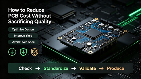
How-To: Find PCB Cost Savings Before Ordering
A practical review can be completed in several steps.
Step 1: Check the Layer Count
Ask:
Can the board meet its routing and signal requirements with fewer layers?
If yes, evaluate the alternative stackup.
Do not reduce layers automatically.
Step 2: Review the Material
Ask:
Does the design actually require a specialized laminate?
If standard FR-4 meets the requirements, compare it against the current material.
Step 3: Review the Via Structure
Look for:
- Blind vias
- Buried vias
- Microvias
- Stacked microvias
- Via-in-pad
Determine which structures are essential.
Step 4: Check Copper Weight
Identify the actual current requirements for each layer.
Avoid using heavy copper where it does not provide a useful electrical benefit.
Step 5: Review Board Dimensions
Check whether a small change in board outline could improve panel utilization.
Step 6: Review Surface Finish
Confirm that the selected finish is required by the assembly process.
Step 7: Review Tolerances
Separate genuinely critical dimensions from specifications that could use standard tolerances.
Step 8: Compare Complete Quotes
When comparing quotations, use the same:
- Material
- Layer count
- Copper weight
- Surface finish
- Quantity
- Testing
- Lead time
Otherwise, a lower quotation may simply be based on a different specification.
What Should You Never Cut Just to Reduce PCB Cost?
Some specifications are directly related to product performance or reliability.
Be particularly careful about reducing:
Copper Thickness
If the electrical design requires a specific current capacity, reducing copper can increase resistance and heating.
Plating Requirements
Insufficient via plating can affect long-term reliability.
Material Performance
Using an unsuitable laminate can create thermal or signal-integrity problems.
Required Testing
Removing appropriate inspection can increase the risk of defective boards entering assembly.
Critical Tolerances
If a mechanical or electrical interface genuinely requires a tolerance, relaxing it can create downstream failures.
Cost optimization should happen around these requirements, not by simply removing them.
A Practical PCB Cost Optimization Example
Consider an 8 layer PCB with:
- High-Tg material
- 2 oz copper on every layer
- ENIG
- Microvias
- Via-in-pad
- Tight trace spacing
- Tight dimensional tolerances
The first reaction might be to ask for a cheaper PCB manufacturer.
A better approach is to review the design.
Suppose the engineering review shows:
- Only two layers actually require 2 oz copper
- Standard FR-4 meets the thermal requirements
- Several microvias can be replaced with through-hole vias
- Via-in-pad is only necessary beneath one BGA
- Some dimensional tolerances can use standard values
The revised design may have substantially lower manufacturing complexity.
The savings come from design optimization, not from compromising the finished PCB.
PCB Cost vs Total Product Cost
A PCB is only one part of the finished electronic product.
A slightly cheaper PCB can become more expensive if it causes:
- SMT defects
- Rework
- Longer assembly time
- Signal debugging
- Thermal problems
- Field failures
For this reason, PCB cost should be evaluated together with:
fabrication + assembly + testing + inventory + reliability
This is especially important when the PCB is used in industrial or long-life products.
FAQ
A: Start with layer count, board dimensions, panel utilization, material selection, via structure, and unnecessary tolerances. These areas often provide more meaningful savings than simply negotiating the unit price.
A: No. A lower layer count can create routing difficulties, increase board size, or require more expensive fabrication features. The complete design should be evaluated.
A: Only when the cheaper material still meets the electrical, thermal, mechanical, and reliability requirements.
A: Not if the testing is required to control product risk. Testing should be matched to the application rather than eliminated solely for a lower quotation.
A: No. HDI costs more to fabricate, but it can reduce board size or avoid a much higher conventional layer count. The correct comparison is between complete design alternatives.
Conclusion
The most effective PCB cost reductions usually happen before the production order is placed.
Instead of asking only how to obtain a lower unit price, review the design for unnecessary manufacturing complexity.
The most useful areas to examine are:
- Layer count
- Stackup
- Material
- Copper weight
- Via structure
- Board dimensions
- Panel utilization
- Trace geometry
- Tolerances
- Surface finish
- Production quantity
The objective is simple:
remove unnecessary cost, not necessary quality.
A well-optimized PCB should be straightforward to manufacture, meet the electrical and mechanical requirements, and avoid processes that exist only because they were specified without a clear engineering reason.
For projects handled by TOPFAST, the same review can be performed before fabrication so that potential cost drivers are identified while changes are still practical.
 EN
EN  PT
PT  AR
AR  DE
DE  FR
FR  ES
ES