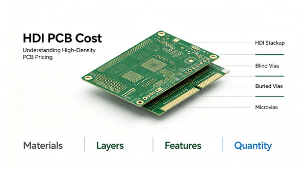
HDI technology is often introduced when a conventional multilayer PCB can no longer provide enough routing density within the available board area.
It is particularly useful for designs containing:
- Fine-pitch BGAs
- High pin-count processors
- Compact modules
- High-density connectors
- Mobile or portable electronics
- Dense high-speed circuits
The trade-off is manufacturing complexity.
An HDI PCB can require laser drilling, microvia formation, sequential lamination, copper filling, and tighter registration control.
As a result, an HDI board is generally more expensive than a conventional PCB with a similar external size and layer count.
However, HDI does not have one fixed price level.
A simple 1+N+1 construction and a more complex stacked-microvia design can have very different manufacturing costs.
Table of Contents
What Makes HDI PCB Manufacturing More Expensive?
The main difference between conventional multilayer fabrication and HDI is the additional manufacturing structure.
Depending on the design, HDI production may involve:
- Laser drilling
- Microvia plating
- Sequential lamination
- Via filling
- Additional imaging
- Additional registration control
- More complex inspection
These processes add both material and manufacturing time.
The cost therefore depends heavily on the actual HDI construction rather than simply the number of PCB layers.
HDI Structure Has a Direct Impact on Cost
There are several ways to construct an HDI PCB.
Common configurations include:
- 1+N+1
- 2+N+2
- 3+N+3
- Any-layer HDI
The notation describes the number of sequentially laminated HDI layers around the core.
For example, a 1+N+1 structure is generally simpler than a 2+N+2 construction.
As the number of sequential lamination cycles increases, manufacturing becomes more complicated.
This is one of the reasons why two HDI boards with the same overall layer count can have significantly different prices.
Microvias Are One of the Main Cost Drivers
Microvias are normally formed using laser drilling rather than conventional mechanical drilling.
Their advantages include:
- Smaller diameter
- Higher routing density
- Shorter electrical path
- Better compatibility with fine-pitch packages
But laser drilling introduces another manufacturing process.
The cost is affected by:
- Number of microvias
- Via diameter
- Via density
- Microvia structure
- Filled or unfilled vias
- Stacked or staggered configuration
A board containing a small number of relatively simple microvias may be much easier to manufacture than one relying heavily on stacked microvias.
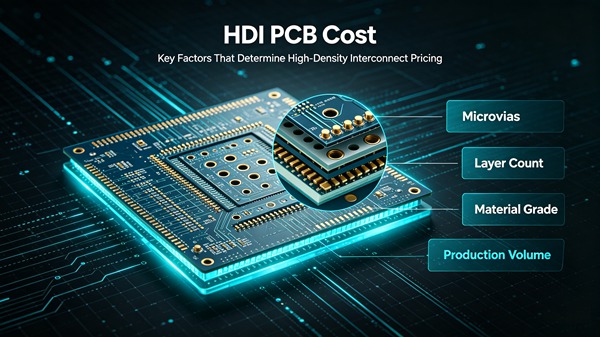
Stacked vs Staggered Microvias
Microvias can be arranged in different ways.
Staggered Microvias
Each microvia is offset from the one below it.
This can simplify some manufacturing requirements.
Stacked Microvias
Microvias are positioned directly above one another.
Stacked structures can provide greater routing flexibility, especially in dense areas.
However, they require tighter process control and may require copper filling.
That additional processing can increase cost.
For this reason, stacked microvias should normally be used where the layout actually requires them.
Sequential Lamination Adds Cost
Conventional multilayer PCBs can often be produced using a comparatively straightforward lamination sequence.
HDI may require multiple lamination cycles.
A simplified process can look like:
Core fabrication → lamination → laser drilling → plating → additional lamination → laser drilling → plating
Each additional cycle adds:
- Material
- Processing time
- Registration requirements
- Inspection requirements
The more complex the sequential structure, the greater the potential manufacturing cost.
Via Filling Can Increase the Price
Some HDI designs require filled microvias.
Copper-filled vias are commonly used for:
- Stacked microvias
- Via-in-pad
- Fine-pitch BGA applications
The filling process requires additional process control.
For a simple routing structure, leaving a microvia unfilled may be sufficient.
For a dense BGA area, however, via filling may be necessary to make the layout manufacturable.
The cost should therefore be evaluated against the packaging requirements.
Via-in-Pad Is Not Always Necessary
Via-in-pad can provide substantial routing benefits.
It allows vias to be placed directly within component pads, reducing the space required for fanout.
This is particularly useful for fine-pitch BGAs.
However, via-in-pad may require:
- Filled vias
- Planarized surfaces
- Additional processing
If a conventional fanout can achieve the same result, avoiding via-in-pad may reduce manufacturing complexity.
BGA Pitch Can Drive HDI Cost
Component pitch has a direct relationship with routing density.
A relatively large-pitch BGA may be routed using conventional vias.
A fine-pitch BGA may require microvias and via-in-pad structures.
For example, moving from a conventional BGA to a much finer-pitch package can change the entire PCB fanout strategy.
This is why HDI decisions should be made together with component selection.
Board Size Is One of the Reasons to Use HDI
At first glance, HDI seems like a cost-increasing technology.
But it can also reduce the total product cost by allowing the PCB to become smaller.
A smaller board may reduce:
- Enclosure size
- Material usage
- Product weight
- Connector spacing
- Assembly footprint
For compact products, the additional HDI fabrication cost can therefore be justified by the reduction in product size.
Layer Count and HDI Cost
HDI and layer count are related, but they are not the same thing.
An 8 layer HDI PCB is not necessarily cheaper than a 10 layer conventional PCB.
The correct comparison should consider the entire structure.
For example:
Option A
- 10 conventional layers
- Through-hole vias
- Larger board
Option B
- 8 layers
- HDI
- Microvias
- Smaller board
Option B may have a higher PCB unit price while still producing a better overall product.
This is why PCB cost should be evaluated at the system level.
The same principle applies when comparing different multilayer constructions in 8 Layer PCB Cost.
Material Selection
Many HDI boards use standard FR-4 or high-Tg FR-4.
More demanding applications may require specialized materials.
Material selection affects:
- Lamination behavior
- Thermal expansion
- Signal integrity
- Reliability
- Processing window
For high-speed HDI designs, the material’s electrical properties may be more important than a relatively small difference in laminate price.
Copper Thickness
HDI structures generally use relatively fine copper features.
The copper thickness must balance:
- Current requirements
- Trace geometry
- Etching capability
- Via reliability
Heavy copper and extremely fine HDI routing can be difficult to combine.
If high-current paths are present, the stackup may need to separate power requirements from fine-pitch routing requirements.
HDI PCB Cost by Design Complexity
A useful way to think about HDI pricing is by structure rather than a fixed price range.
| HDI Structure | Relative Complexity |
|---|---|
| 1+N+1 | Lower |
| 2+N+2 | Moderate |
| 3+N+3 | Higher |
| Stacked microvias | Higher |
| Via-in-pad | Higher |
| Any-layer HDI | Very high |
These categories are only a relative guide.
The actual quotation also depends on board size, material, quantity, copper structure, and production requirements.
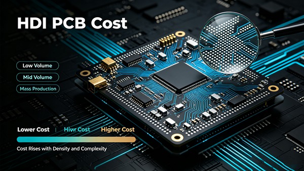
How-To: Reduce HDI PCB Cost
Step 1: Confirm That HDI Is Actually Necessary
Start with the BGA fanout and routing density.
If the design can be completed using conventional vias without increasing board size excessively, conventional multilayer fabrication may be more economical.
Step 2: Choose the Simplest HDI Structure
If 1+N+1 can meet the requirements, there may be little reason to use a more complicated sequential structure.
The objective is not to maximize HDI capability.
It is to solve the routing problem with the simplest reliable construction.
Step 3: Minimize Stacked Microvias
Use staggered microvias where the layout allows it.
Stacked structures should be reserved for areas where they provide a clear routing benefit.
Step 4: Use Via-in-Pad Selectively
Do not place filled microvias in every BGA pad unless the package fanout actually requires it.
Step 5: Review BGA Selection
Sometimes a slightly different package pitch can significantly simplify PCB fabrication.
This is a design decision that should be made before PCB layout is finalized.
Step 6: Optimize Board Dimensions
If HDI allows the board to become significantly smaller, compare the additional PCB fabrication cost against the reduction in overall product size.
When Is HDI Worth the Additional Cost?
HDI is usually justified when it solves a physical design problem that conventional fabrication cannot solve efficiently.
Typical examples include:
Fine-Pitch BGA
The package has insufficient space for conventional via fanout.
Compact Product
The board must fit within a small mechanical enclosure.
High Routing Density
There are too many connections for conventional layer structures.
High-Speed Design
Microvias can provide shorter connections and more controlled routing structures.
Layer Reduction
HDI may allow the designer to achieve the required routing density without adding many conventional layers.
When HDI May Be Unnecessary
HDI may not be the best choice when:
- Board space is available
- Components have relatively large pitch
- Conventional vias provide sufficient routing
- The product has no significant size constraint
- A standard multilayer stackup meets signal requirements
In these cases, conventional multilayer fabrication may offer a better cost-to-complexity ratio.
HDI Cost Should Be Compared With the Alternativ
A useful engineering comparison is:
Conventional PCB
Lower fabrication complexity
- Larger board
- More layers or routing compromises
versus:
HDI PCB
Higher fabrication complexity
- Smaller board
- Better routing density
The right answer depends on the product.
If the PCB is a small part of a much larger system, reducing the board footprint may justify a higher PCB price.
If the enclosure has plenty of space, paying for HDI may provide little practical benefit.
FAQ
A: Generally yes. Laser drilling, sequential lamination, microvia processing, and other additional operations increase manufacturing complexity.
A: A relatively simple 1+N+1 construction is generally less complex than 2+N+2, 3+N+3, or any-layer structures, assuming other specifications are comparable.
A: No. Staggered microvias can be sufficient for many designs. Stacked structures are used when routing density or package requirements justify them.
A: It can. Filled and planarized vias require additional processing, so via-in-pad should be used where it provides a real layout benefit.
A: Yes. Although the PCB itself may cost more, HDI can reduce board size, enclosure dimensions, layer count, and sometimes assembly complexity.
Conclusion
HDI increases PCB manufacturing cost because it introduces processes that are not required for conventional multilayer boards.
The biggest cost drivers are usually:
- Sequential lamination
- Microvias
- Stacked microvias
- Via filling
- Via-in-pad
- Fine-pitch routing
- Specialized materials
But avoiding HDI simply because it costs more is not always the right decision.
If HDI allows a smaller board, simplifies a fine-pitch BGA layout, or avoids a much higher conventional layer count, the additional fabrication cost may be justified.
The practical approach is to start with the package, routing density, board dimensions, and electrical requirements, then select the simplest HDI structure that solves the actual design problem.
For TOPFAST projects involving complex HDI structures, the stackup and via strategy should ideally be reviewed before final Gerber release. That makes it easier to identify unnecessary process steps before they become part of the production cost.
 EN
EN  PT
PT  AR
AR  DE
DE  FR
FR  ES
ES