An 8 layer PCB is usually considered when a 4 or 6 layer design can no longer provide enough routing space or adequate electrical performance.
It is commonly used in:
- Networking equipment
- Industrial control systems
- Embedded computing
- Communication products
- High-speed digital electronics
- Automotive electronics
- Complex instrumentation
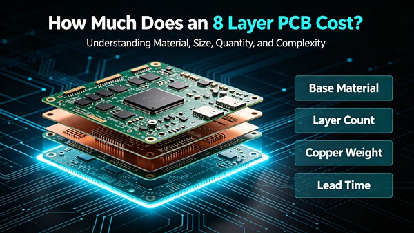
The price of an 8 layer PCB depends on much more than the number of layers.
Important variables include:
- Board dimensions
- Stackup
- Laminate selection
- Copper weight
- Minimum trace and spacing
- Via structure
- Impedance requirements
- Surface finish
- Quantity
- Testing
- Production lead time
An 8 layer board with conventional FR-4 and through-hole vias can have a very different manufacturing cost from an 8 layer HDI board using sequential lamination and microvias.
Table of Contents
Why Does an 8 Layer PCB Cost More?
The additional layers increase both material consumption and manufacturing operations.
Compared with a conventional 4 layer board, an 8 layer construction generally requires more:
- Core material
- Prepreg
- Copper foil
- Inner-layer processing
- Lamination
- Drilling
- Plating
- Registration control
- Inspection
However, the cost does not simply increase in proportion to layer count.
Production quantity and panel utilization can significantly change the unit price.
For example, a small prototype batch may have a relatively high unit cost because engineering and setup costs are distributed across only a few boards.
At production quantities, those fixed costs have a much smaller effect on each PCB.
Stackup Is a Major Cost Consideration
An 8 layer PCB gives engineers considerably more flexibility when arranging signal, power, and ground layers.
A simplified construction might look like:
L1 SignalL2 GroundL3 SignalL4 PowerL5 GroundL6 SignalL7 Ground / PowerL8 Signal
The actual stackup depends on the design.
For high-speed applications, the stackup must also account for:
- Controlled impedance
- Signal return paths
- Crosstalk
- Plane continuity
- Dielectric thickness
- Material Dk
This means that the cheapest possible stackup is not always the most appropriate one.
A poorly planned stackup can create signal-integrity problems that are much more expensive to fix after fabrication.
A detailed discussion of these relationships is covered in PCB Stackup Design.
Material Selection Can Change the Price Significantly
Standard FR-4 is sufficient for many 8 layer boards.
But some applications require higher-performance laminates.
Examples include:
- High-Tg FR-4
- Low-loss laminates
- High-frequency materials
- Low-CTE materials
For a conventional industrial controller, standard FR-4 may be perfectly adequate.
For a high-speed networking board, dielectric loss and Dk stability can become much more important.
The material should therefore be selected according to the actual electrical and environmental requirements.
Using an expensive material without a technical reason adds cost without necessarily improving the product.
Board Size and Panel Utilization
Board area directly affects material consumption, but panel utilization also matters.
Consider two designs with almost identical dimensions.
If one layout allows more individual boards to fit efficiently on a production panel, the material cost per PCB may be lower.
This is particularly relevant for production quantities.
When the mechanical design is still flexible, it can be worthwhile to review:
- Board outline
- Array arrangement
- Rail requirements
- Tooling areas
before releasing the final manufacturing data.
Copper Weight
Many 8 layer PCBs use standard copper weights, but power-intensive designs may require heavier copper on selected layers.
Higher copper weight increases:
- Material usage
- Plating requirements
- Etching difficulty
- Process control requirements
If a design has both high-current and low-current layers, it may be worth evaluating whether all layers actually need the same copper weight.
The objective is not to minimize copper at any cost, but to avoid specifying more copper than the electrical design requires.
Via Structure Has a Major Impact
This is one of the areas where two 8 layer PCBs can become very different in price.
A conventional design may use standard through-hole vias.
Another design may require:
- Blind vias
- Buried vias
- Microvias
- Via-in-pad
- Backdrilling
Each additional structure introduces manufacturing requirements.
Through-Hole Vias
These are generally the simplest option.
Blind and Buried Vias
These can improve routing flexibility but require more complex fabrication.
Microvias
Microvias are commonly associated with HDI designs and laser drilling.
Backdrilling
Backdrilling can remove unused portions of plated through-holes and improve high-speed signal performance.
It adds another manufacturing operation and therefore needs to be justified by the electrical design.
For more complex structures, see the existing HDI PCB content.
Controlled Impedance Can Affect Cost
An 8 layer board is often used for designs with multiple high-speed interfaces.
Examples include:
- DDR memory
- PCIe
- Ethernet
- USB
- SerDes
- RF-related interfaces
These designs may require controlled impedance.
The impedance requirement affects the PCB construction through:
- Trace width
- Copper thickness
- Dielectric thickness
- Reference plane position
- Material properties
A tighter impedance tolerance can require more process control and verification.
It is therefore important to specify the impedance requirements before the stackup is finalized.
Surface Finish
Surface finish usually has less influence on the total cost than layer count or special via structures, but it still contributes to the quotation.
Typical choices include:
- HASL
- Lead-free HASL
- ENIG
- OSP
- Immersion silver
The selection should be based on:
- Component pitch
- Assembly process
- Product environment
- Reliability requirements
For example, a fine-pitch BGA design may benefit from a flatter surface finish.
PCB Thickness
An 8 layer PCB does not automatically require a thick board.
The final thickness depends on:
- Core thickness
- Prepreg construction
- Copper thickness
- Mechanical requirements
- Impedance requirements
If the enclosure permits a standard construction, there may be no reason to specify an unusual thickness.
However, high-speed designs sometimes require a specific dielectric geometry to achieve the desired impedance.
In those cases, electrical requirements take priority over a small difference in material cost.
Why HDI Can Make an 8 Layer PCB Much More Expensive
An 8 layer PCB does not necessarily mean HDI.
A conventional 8 layer board can often be fabricated using through-hole technology.
HDI becomes useful when the design has problems such as:
- Very dense BGA packages
- Limited board area
- Fine-pitch components
- Large numbers of connections
- Difficult inner-layer routing
HDI may introduce:
- Laser drilling
- Microvia filling
- Sequential lamination
- Additional plating
- Tighter registration requirements
If the design can be successfully routed without these processes, avoiding unnecessary HDI structures can reduce cost.
How-To: Review an 8 Layer PCB Cost Before Production
Step 1: Confirm the Layer Structure
Do not simply specify “8 layers.”
Define what each layer is doing.
For example:
L1 – SignalL2 – GroundL3 – SignalL4 – PowerL5 – GroundL6 – SignalL7 – Power / GroundL8 – Signal
The actual stackup should be developed around the electrical requirements.
Step 2: Check the Material
Confirm:
- Laminate family
- Tg
- Dk/Df where relevant
- Core and prepreg construction
Step 3: Review the Via Strategy
Ask whether the design really needs:
- Microvias
- Blind vias
- Buried vias
- Backdrilling
If standard through-hole vias work, they can simplify fabrication.
Step 4: Check Impedance Requirements
Identify:
- Single-ended impedance
- Differential impedance
- Required tolerance
- High-speed interfaces
These requirements should be considered before stackup finalization.
Step 5: Review Copper Weight
Identify which layers actually carry significant current.
Avoid automatically specifying heavy copper across the entire board.
Step 6: Compare Equivalent Quotes
Make sure different quotations use the same:
- Material
- Stackup
- Copper weight
- Surface finish
- Quantity
- Testing requirements
- Lead time
Otherwise, the price comparison is misleading.
When Is an 8 Layer PCB Worth the Extra Cost?
Moving from 6 to 8 layers makes sense when the additional routing capacity solves a real design problem.
Typical reasons include:
More High-Speed Routing
Additional layers provide more routing channels and reference planes.
Better Power Distribution
Separate power and ground structures can simplify distribution.
Reduced Crosstalk
Better layer assignment and reference-plane control can improve signal isolation.
Fewer Routing Compromises
A higher layer count may allow wider traces and cleaner routing.
Smaller Board Size
Adding layers can sometimes allow the PCB to become smaller.
This is an important trade-off.
A larger 6 layer board may not necessarily be cheaper for the complete product than a smaller 8 layer board.
8 Layer PCB Cost vs 6 Layer PCB Cost
The difference should not be viewed only as:
8 layers = more expensive
The more useful comparison is:
| Design Aspect | 6 Layer | 8 Layer |
|---|---|---|
| Routing capacity | Moderate | Higher |
| Reference planes | Good | More flexible |
| High-speed routing | Moderate | Better |
| Material usage | Lower | Higher |
| Fabrication complexity | Moderate | Higher |
| HDI requirement | Application dependent | Application dependent |
| Typical design density | Medium | Medium–high |
For a simple controller, 8 layers may be unnecessary.
For a dense computing or networking design, the additional layers can simplify the entire PCB.
How to Reduce 8 Layer PCB Cost
The most practical approach is to reduce unnecessary process complexity.
Use a Conventional Construction When Possible
If through-hole vias can meet the routing requirements, there may be no reason to introduce microvias.
Use Standard Materials When Appropriate
Specialized low-loss materials should be reserved for designs that actually need them.
Avoid Excessive Copper
Use heavier copper where current and thermal requirements justify it.
Optimize Board Dimensions
A better outline can improve panel utilization.
Review Impedance Requirements Early
Late stackup changes can result in redesign and additional engineering work.
Avoid Unnecessarily Tight Tolerances
Designing close to the manufacturing limit can increase production difficulty without providing a real product benefit.
FAQ
A:It generally costs more than a comparable 4 or 6 layer board because of additional material and fabrication steps. However, the actual price depends heavily on the stackup, material, board size, quantity, and via structure.
A: Common reasons include higher routing density, more high-speed interfaces, improved power distribution, better reference-plane control, and reduced board size.
A: No. Many 8 layer boards can be manufactured using conventional through-hole vias. HDI is used when routing density or component packaging requires it.
A: Yes. Standard FR-4 is suitable for many applications. High-speed or demanding environments may require a different material system.
A: The combination of material, board size, quantity, stackup, copper weight, via structure, and special fabrication processes usually has a much greater effect than any single specification
Conclusion
An 8 layer PCB costs more than a simpler multilayer board because it requires additional material and fabrication operations. But the additional layers can provide substantial engineering benefits.
The decision should be based on what the extra layers solve.
If they provide:
- Better signal integrity
- More routing capacity
- Cleaner power distribution
- Improved reference planes
- A smaller board
then the additional fabrication cost may be justified.
For cost control, the best approach is to keep the construction as simple as the design allows:
appropriate stackup + suitable material + practical via structure + reasonable tolerances
That gives engineers a more useful target than simply trying to obtain the lowest possible PCB quotation.
 EN
EN  PT
PT  AR
AR  DE
DE  FR
FR  ES
ES