• Have any question ?+86 139 2957 6863
  • Send emailop@topfastpcb.com

Get a Quote

8 Layer PCB Manufacturing

by Topfast | Sunday Jul 05 2026

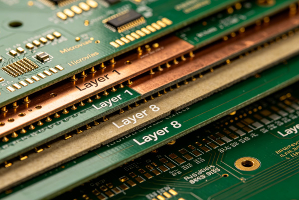
As electronic products become smaller and more powerful, PCB designs require more routing layers and better electrical performance. An 8 layer PCB provides additional signal layers, dedicated reference planes, and improved power distribution compared with 4-layer and 6-layer boards.

8-layer PCBs are widely used in:

  • Industrial automation
  • Communication systems
  • High-speed digital circuits
  • Automotive electronics
  • Medical equipment
  • Embedded computing platforms
  • Networking devices
  • AI and server hardware

TOPFAST provides custom 8 layer PCB manufacturing with support for controlled impedance, high Tg materials, and prototype to volume production.

Why Choose an 8 Layer PCB?

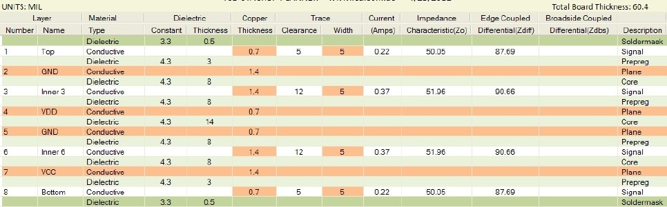
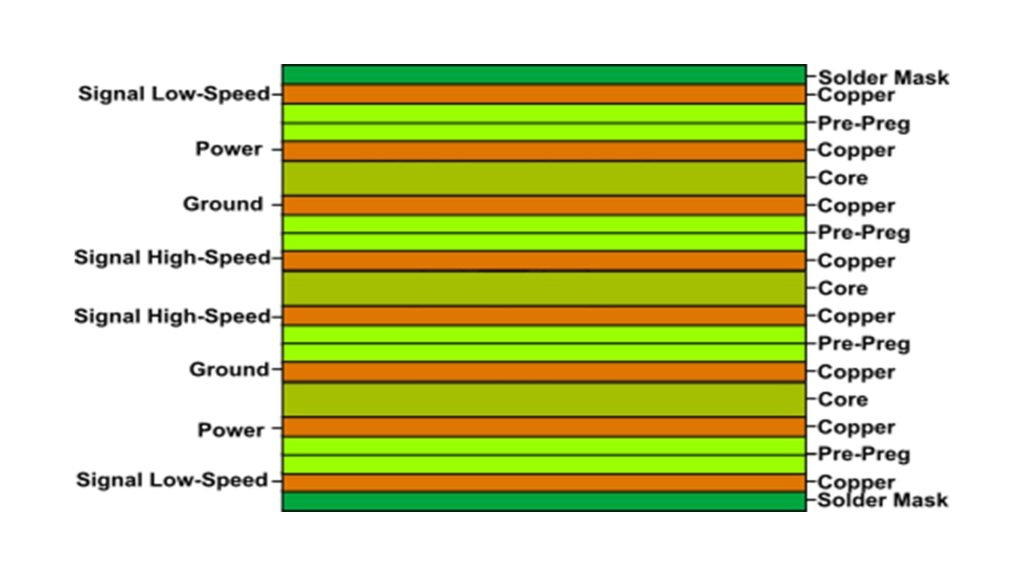
Compared with lower layer count boards, 8 layer structures offer significant electrical and mechanical advantages.

Improved Signal Integrity

Additional ground and power planes help:

  • Reduce crosstalk
  • Improve return paths
  • Minimize signal reflections
  • Enhance impedance stability

This is especially important for:

  • DDR memory
  • PCIe interfaces
  • Ethernet
  • USB 3.0 and USB4

Higher Routing Density

Eight layers provide more routing channels, allowing:

  • Compact board dimensions
  • Higher component density
  • Complex processor designs
  • BGA package support

Better EMI Performance

Dedicated reference planes reduce:

  • Electromagnetic radiation
  • Switching noise
  • Signal coupling

Internal Link: PCB Stackup Design Guide

Improved Reliability

Balanced multilayer structures help minimize:

  • Warpage
  • Mechanical stress
  • Thermal deformation

Related Reading: PCB Warpage and Reflow Deformation

Typical 8 Layer PCB Stackup

A common 8-layer stackup is:

Layer 1   Signal
Layer 2 Ground
Layer 3 Signal
Layer 4 Power
Layer 5 Ground
Layer 6 Signal
Layer 7 Ground
Layer 8 Signal

Benefits include:

  • Excellent signal integrity
  • Controlled impedance
  • Low EMI
  • Stable power distribution

Alternative stackups may be optimized for:

  • High-speed digital systems
  • RF circuits
  • Power electronics
  • HDI designs

Related Reading: High Frequency PCB Material Selection

Standard 8 Layer PCB Specifications

ParameterCapability
Layer Count8 Layers
MaterialFR4, High Tg, Rogers
Copper Weight0.5–4 oz
Board Thickness0.4–3.2 mm
Min Trace/Space3/3 mil
Min Drill Size0.15 mm
Surface FinishHASL, ENIG, OSP, Immersion Silver
Impedance ControlAvailable
IPC StandardIPC Class 2 / Class 3

Material Options for 8 Layer PCBs

Standard FR4

Suitable for:

  • Industrial electronics
  • Consumer products
  • Embedded controllers

Advantages:

  • Low cost
  • High mechanical strength
  • Mature manufacturing process

High Tg Materials

Recommended for:

  • Automotive electronics
  • High-temperature environments
  • Lead-free assembly

Benefits include:

  • Better thermal stability
  • Improved reliability
  • Reduced delamination risk

Internal Link: PCB Delamination Causes and Prevention

Rogers Materials

Suitable for:

  • RF applications
  • High-speed communication
  • Microwave circuits

Common materials include:

  • RO4350B
  • RO4003C
  • RO3003

Related Reading: High Frequency PCB Material Selection

Applications of 8 Layer PCBs

Networking Equipment

8-layer boards are widely used in:

  • Switches
  • Routers
  • Optical communication modules

Their additional layers support:

  • Differential pair routing
  • Controlled impedance
  • Signal integrity optimization

Industrial Automation

Industrial products require:

  • High reliability
  • Long service life
  • Stable electrical performance

Automotive Electronics

Applications include:

  • ECU modules
  • ADAS controllers
  • Battery management systems

Related Reading: Automotive PCBA Reliability Design

Medical Equipment

Medical systems demand:

  • Signal stability
  • Low noise
  • High reliability

AI Servers and Embedded Computing

Complex processors and memory architectures require:

  • Dense routing
  • Multiple reference planes
  • High-speed signal integrity

Key Design Considerations

PCB Stackup Design

Stackup planning determines:

  • Signal integrity
  • Power integrity
  • EMI performance
  • Manufacturability

Internal Link: PCB Stackup Design Guide

Controlled Impedance

Many interfaces require controlled impedance:

InterfaceTypical Impedance
USB90 Ω Differential
Ethernet100 Ω Differential
PCIe85 Ω Differential
DDR40–60 Ω Single Ended

Via Reliability

As layer count increases, via quality becomes increasingly important.

Design considerations include:

  • Aspect ratio
  • Copper plating thickness
  • Thermal expansion

Related Reading: PCB Via Failure Analysis

Copper Balance

Uneven copper distribution can lead to:

  • Bow and twist
  • Internal stress
  • Delamination

Proper copper balancing improves long-term reliability.

How to Order an 8 Layer PCB

  1. Step 1

    Provide:
    . Gerber files
    . Stackup information
    . Impedance requirements

  2. Step 2

    Select:
    . Material type
    . Copper thickness
    . Surface finish

  3. Step 3

    Engineering review and DFM analysis.

  4. Step 4

    Prototype verification.

  5. Step 5

    Mass production.

Need Custom 8 Layer PCB Manufacturing?

TOPFAST supports:

✓ High Tg and Rogers materials

✓ Controlled impedance structures

✓ IPC Class 2 and IPC Class 3 production

✓ Prototype and volume manufacturing

✓ Engineering review and DFM support

Frequently Asked Questions

Q: What are 8 layer PCBs used for?

A: 8 layer PCBs are commonly used in networking equipment, industrial automation, automotive electronics, AI servers, and medical devices.

Q: Is an 8 layer PCB better than a 6 layer PCB?

A: An 8 layer PCB provides more routing space, improved EMI performance, and better signal integrity for complex designs.
Related Reading: 6 Layer PCB Manufacturing

Q: What is the standard thickness of an 8 layer PCB?

A: Common thicknesses include:
. 1.2 mm
. 1.6 mm
. 2.0 mm
Custom thicknesses are also available.

Q: Can an 8 layer PCB support high-speed signals?

A: Yes. Eight-layer structures are widely used for PCIe, DDR, Ethernet, and other high-speed interfaces.

Q: Which materials are commonly used for 8 layer PCBs?

A: Standard FR4, High Tg FR4, and Rogers laminates are the most common options.

Conclusion

An 8 layer PCB offers an excellent combination of routing density, signal integrity, EMI performance, and reliability.

With dedicated power and ground planes, optimized stackups, and advanced materials, 8-layer boards support increasingly complex electronic products ranging from industrial automation to high-speed networking and AI computing.

Through proper stackup design, impedance control, and manufacturing process optimization, 8 layer PCBs provide reliable performance throughout the product lifecycle.

Latest Posts

View More
Contact us
Talk to Our PCB Expert
en_USEN