In modern electronics, vias are among the most important structures inside a printed circuit board.
Whether connecting power planes, signal layers, or ground networks, vias provide the electrical pathways that enable multilayer PCB functionality.
When a via fails, the result can be difficult to diagnose. Unlike obvious component failures, via defects often create intermittent problems that appear only under temperature changes, vibration, or long-term operation.
Understanding via failure mechanisms is essential for improving PCB reliability, particularly in automotive, industrial, aerospace, and power electronics applications.
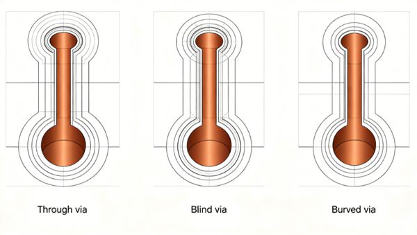
Table of Contents
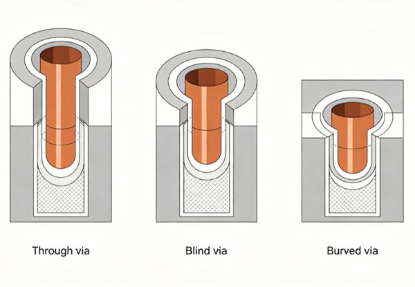
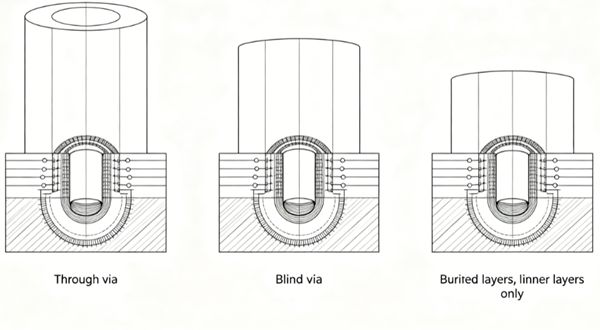
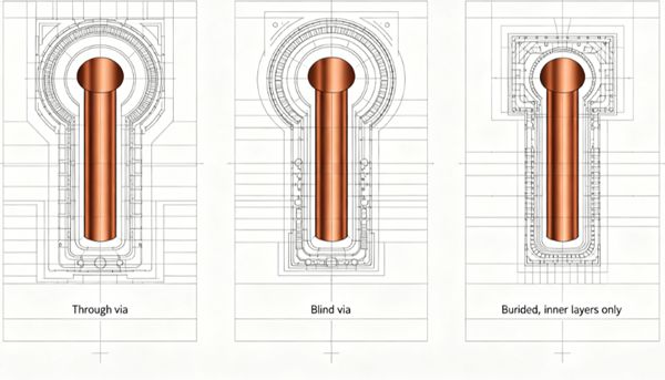
What Is a PCB Via?
A PCB via is a plated hole that electrically connects different layers of a circuit board.
Common via types include:
- Through-hole vias
- Blind vias
- Buried vias
- Microvias
These structures allow signals and power to travel between layers while supporting increasingly complex PCB designs.
Related Reading: HDI PCB Technology Guide
Why Via Reliability Matters
Modern electronic systems may contain thousands of vias.
A single failed via can cause:
- Open circuits
- Intermittent electrical connections
- Communication failures
- Power instability
- Complete product malfunction
As layer counts increase, via reliability becomes one of the most important factors affecting PCB lifespan.
Internal Link: Multilayer PCB Supplier
Common PCB Via Failure Mechanisms
Barrel Cracking
Barrel cracking is one of the most frequently observed failures.
The copper plating inside the hole wall develops cracks due to mechanical or thermal stress.
Common causes include:
- Thermal cycling
- Excessive Z-axis expansion
- Poor plating thickness
- Material mismatch
Barrel cracks often appear after long-term field operation rather than immediately after production.
Corner Cracking
Corner cracking occurs where the via barrel meets internal copper pads.
Stress concentrations develop at these locations during:
- Reflow soldering
- Thermal shock
- Power cycling
Repeated expansion and contraction eventually cause copper fatigue.
Via Separation
Via separation occurs when the plated copper loses contact with the inner-layer pad.
Potential causes include:
- Poor drilling quality
- Misregistration
- Insufficient plating
- Lamination defects
This failure often creates intermittent electrical behavior.
Related Reading: PCB Delamination Causes and Prevention
Plating Voids
Voids occur when electroplating fails to deposit copper throughout the via structure fully.
Common causes include:
- Contamination
- Improper chemistry control
- Poor solution circulation
- Inadequate process monitoring
Even small voids can significantly reduce via reliability.
Microvia Failure
HDI boards frequently use laser-drilled microvias.
Common microvia defects include:
- Via cracking
- Incomplete copper filling
- Interface separation
- Stacked-via fatigue
As operating temperatures increase, microvia reliability becomes increasingly important.
Internal Link: HDI PCB Supplier
Root Causes of PCB Via Failures
Thermal Expansion Mismatch
Different PCB materials expand at different rates.
Key materials include:
- Copper
- Resin systems
- Glass fiber reinforcement
Repeated expansion and contraction generate mechanical stress within the via structure.
Excessive Assembly Temperatures
Lead-free soldering processes typically exceed:
245°C–260°CRepeated thermal exposure accelerates copper fatigue and via degradation.
Internal Link: PCB Warpage and Reflow Deformation
Insufficient Copper Thickness
Thin plating significantly reduces fatigue resistance.
Industry standards generally require a minimum plating thickness to ensure long-term reliability.
Poor process control may produce:
- Weak via barrels
- Reduced current-carrying capacity
- Increased crack susceptibility
Poor PCB Material Quality
Low-quality laminates often exhibit:
- High moisture absorption
- Increased expansion rates
- Reduced structural stability
These factors accelerate via stress accumulation.
Improper PCB Design
Design-related issues include:
- Excessive aspect ratios
- Overly small annular rings
- High-density thermal zones
- Poor stackup planning
Design optimization is often the most cost-effective reliability improvement.
How to Detect PCB Via Failures
Cross-Section Analysis
Cross-section inspection remains the most effective failure analysis method.
Engineers can identify:
- Barrel cracks
- Voids
- Separation defects
- Copper thickness issues
Microsection Testing
Microsection analysis provides detailed views of:
- Hole wall quality
- Copper distribution
- Layer connections
This method is widely used during qualification testing.
X-Ray Inspection
X-ray systems can reveal:
- Hidden voids
- Registration issues
- Structural abnormalities
without damaging the board.
Thermal Stress Testing
Thermal stress tests accelerate failure mechanisms through repeated temperature cycling.
Examples include:
- Thermal shock
- Reflow simulation
- Environmental chamber testing
How to Prevent PCB Via Failures
Improve Hole Wall Preparation
Before plating, manufacturers should ensure:
- Proper desmear
- Clean surfaces
- Adequate roughness
This improves copper adhesion.
Increase Copper Plating Quality
Stable plating processes should maintain:
- Uniform thickness
- Consistent grain structure
- Low defect rates
Better plating directly improves fatigue life.
Optimize PCB Stackup Design
Balanced multilayer structures reduce mechanical stress.
Best practices include:
- Symmetrical stackups
- Controlled dielectric thickness
- Even copper distribution
Internal Link: PCB Manufacturing Process
Select Appropriate Materials
High-reliability applications often require:
- High Tg laminates
- Low CTE materials
- Automotive-grade substrates
Conduct Reliability Testing
Qualification testing should include:
- Thermal cycling
- IST testing
- Cross-section verification
- Accelerated life testing
These methods help identify latent via defects before production release.
Industries Most Affected by Via Failures
Automotive Electronics
Vehicle electronics experience:
- Constant vibration
- Thermal cycling
- Long service life requirements
Telecommunications Equipment
High-density boards rely on thousands of vias for signal transmission.
Power Electronics
High-current applications generate significant thermal stress.
Related Reading: Power Electronics PCB Design for EV
Aerospace and Defense
Reliability requirements are extremely demanding due to harsh operating environments.
FAQ
A: Barrel cracking is among the most frequently observed via reliability failures.
A: Thermal cycling causes repeated expansion and contraction that eventually fatigues the copper plating.
A: Via separation occurs when the plated barrel loses electrical connection with an internal layer pad.
A: Using high-quality materials, optimized stackups, proper plating control, and reliability testing significantly improves performance.
A: Microvias can be highly reliable when properly designed and manufactured, but poor process control increases failure risk.
Conclusion
PCB via failures are among the most significant reliability concerns in multilayer circuit boards.
Common failure mechanisms include:
- Barrel cracking
- Corner cracking
- Via separation
- Plating voids
- Microvia fatigue
Through proper design, material selection, process control, and reliability testing, manufacturers can significantly improve performance and extend product lifespan.