
As electronic systems become more powerful and compact, multilayer PCBs have become the standard solution for modern product design.
Compared with simple double-sided boards, multilayer PCBs provide:
- Higher routing density
- Better signal integrity
- Improved power distribution
- More compact product size
However, multilayer fabrication also introduces greater manufacturing complexity. Choosing the right multilayer PCB supplier is critical for ensuring production consistency and long-term reliability.
TOPFAST supports multilayer PCB fabrication with engineering-oriented stack-up review and controlled manufacturing processes for both prototype and production applications.
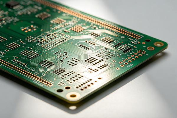
Table of Contents
What Is a Multilayer PCB?
A multilayer PCB contains three or more conductive copper layers laminated together into a single structure.
Common multilayer configurations include:
- 4-layer PCB
- 6-layer PCB
- 8-layer PCB
- 10-layer PCB
- 12-layer and higher-count boards
Multilayer structures are commonly used in:
- Industrial electronics
- Automotive systems
- Networking equipment
- Power electronics
- Communication devices
Why Multilayer PCB Supplier Selection Matters
Multilayer PCB fabrication requires tighter process control than standard two-layer boards.
Potential manufacturing issues include:
- Layer misregistration
- Delamination
- Impedance inconsistency
- Thermal stress deformation
- Poor hole wall reliability
A capable multilayer PCB supplier helps reduce these risks through controlled fabrication and engineering verification.
Key Capabilities of a Multilayer PCB Supplier
1. Stack-Up Engineering
A proper stack-up affects:
- Signal integrity
- EMI performance
- Thermal stability
- Mechanical reliability
Reliable suppliers should support:
- Controlled impedance design
- Symmetrical layer balancing
- Power and ground optimization
Internal Link: PCB Manufacturing Process – Multilayer fabrication involves complex lamination and drilling stages.
2. Layer Registration Accuracy
Precise alignment between layers is essential for:
- Via reliability
- Fine-pitch routing
- Electrical stability
Poor registration can create signal integrity problems and assembly defects.
3. Lamination Process Control
Multilayer boards require controlled pressure and temperature during lamination.
Critical factors include:
- Resin flow management
- Thermal expansion control
- Void prevention
4. Material Selection Capability
Multilayer designs may require:
- Standard FR4
- High Tg materials
- Low-loss laminates
- High-frequency substrates
Material quality directly affects reliability and electrical performance.
5. Hole Reliability and Plating Quality
As the layer count increases, via reliability becomes more critical.
Suppliers should control:
- Copper plating thickness
- Hole wall integrity
- Aspect ratio limitations
Related: HDI PCB Supplier – High-layer-count boards often incorporate HDI structures.
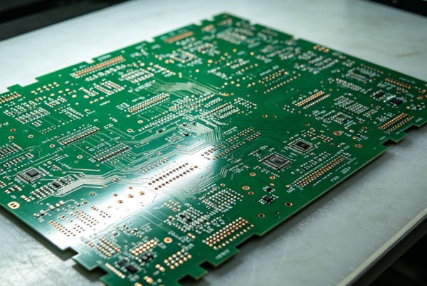
Common Challenges in Multilayer PCB Manufacturing
Warpage and Mechanical Stress
Uneven copper distribution and thermal imbalance may lead to:
- PCB bow and twist
- Reflow deformation
- Assembly instability
Internal Link: PCB Warpage and Reflow Deformation – Common issue in complex multilayer structures.
Signal Integrity Issues
Poor stack-up planning can increase:
- Crosstalk
- EMI
- Impedance variation
Delamination Risk
Improper lamination may cause separation between layers during thermal cycling.
Manufacturing Yield Reduction
Higher layer counts increase fabrication complexity and production risk.
How-To: Choose a Multilayer PCB Supplier
- Step 1: Evaluate Fabrication Capability
Review:
. Maximum layer count support
. Minimum trace and spacing capability
. Controlled impedance experience - Step 2: Review Engineering Support
Strong suppliers should provide:
. Stack-up recommendations
. DFM analysis
. Material optimization guidance - Step 3: Verify Quality Systems
Look for:
. AOI inspection
. Electrical testing
. Cross-section analysis
. Process traceability - Step 4: Assess Thermal and Mechanical Stability
Discuss:
. Warpage control
. Copper balancing strategy
. Lamination reliability - Step 5: Validate Scalability
Ensure the supplier supports:
. Prototype fabrication
. Pilot production
. Stable mass production
Internal Link: Prototype PCB Supplier – Prototype success should transition smoothly into production.
Discuss Your Multilayer PCB Project with TOPFAST – Engineering-focused fabrication for complex PCB designs.
Multilayer PCB vs Double-Sided PCB
| Feature | Double-Sided PCB | Multilayer PCB |
|---|---|---|
| Routing density | Lower | Higher |
| Signal integrity | Moderate | Improved |
| Product size | Larger | More compact |
| Manufacturing complexity | Lower | Higher |
| Cost | Lower | Higher |
| Application complexity | Basic | Advanced |
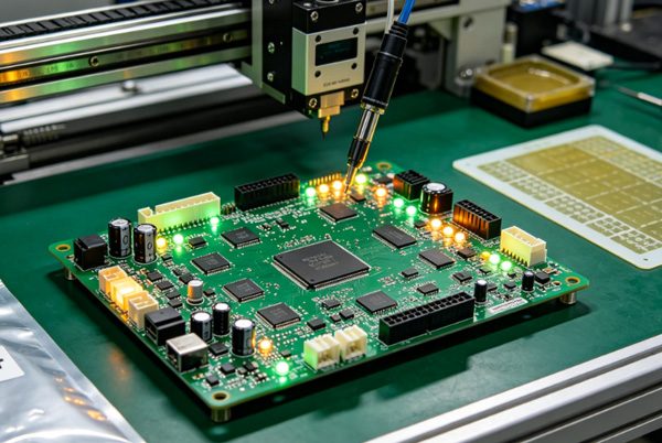
Best Practices for Multilayer PCB Design
- Use symmetrical stack-ups
- Balance copper distribution
- Separate signal and power layers properly
- Minimize unnecessary vias
- Perform fabrication-oriented DFM review early
Frequently Asked Questions (FAQ)
A multilayer PCB supplier manufactures boards with three or more conductive layers.
Additional lamination, drilling, and process control increase manufacturing complexity.
Automotive, communication, industrial, medical, and computing industries commonly use multilayer designs.
Modern PCBs may contain more than 20 layers depending on application requirements.
Maintaining registration accuracy and thermal stability across all layers.
Conclusion
Multilayer PCB fabrication requires advanced process control, engineering expertise, and stable manufacturing systems.
Choosing the right multilayer PCB supplier depends on:
- Stack-up engineering capability
- Material quality
- Registration precision
- Reliability management
- Production scalability
By working with experienced suppliers like TOPFAST, companies can improve multilayer PCB reliability and support more advanced electronic product development.
Request Multilayer PCB Manufacturing Support from TOPFAST – Reliable fabrication for advanced multilayer electronics.
 EN
EN  PT
PT  AR
AR  DE
DE  FR
FR  ES
ES