As electronic products become smaller, faster, and more complex, traditional PCB fabrication methods are often no longer sufficient. Modern electronics increasingly rely on HDI PCB technology to achieve:
- Higher routing density
- Smaller package integration
- Improved signal integrity
- Reduced board size
Selecting the right HDI PCB supplier is critical because HDI manufacturing requires tighter process control, advanced equipment, and specialized engineering expertise.
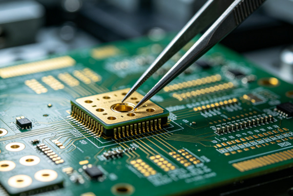
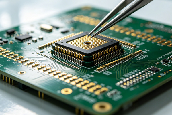
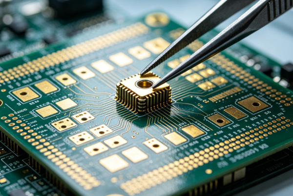
TOPFAST supports HDI PCB fabrication with controlled manufacturing processes and engineering-oriented DFM review to improve production reliability and assembly performance.
Table of Contents
What Is an HDI PCB?
HDI (High-Density Interconnect) PCBs use advanced fabrication techniques such as:
- Microvias
- Blind vias
- Buried vias
- Sequential lamination
- Fine trace routing
HDI structures allow more circuit density within smaller board dimensions.
Typical HDI applications include:
- Smartphones
- Automotive electronics
- Medical devices
- Communication equipment
- Industrial control systems
Why HDI PCB Supplier Selection Matters
HDI fabrication introduces tighter tolerances and more manufacturing complexity than standard multilayer boards.
Small process variations may cause:
- Via a reliability failure
- Layer registration problems
- Impedance inconsistency
- Assembly defects
A capable HDI PCB supplier helps reduce these risks through controlled manufacturing and engineering validation.
Key Capabilities of an HDI PCB Supplier
1. Laser Drilling Capability
Microvias require precise laser drilling systems.
Critical factors include:
- Hole diameter consistency
- Via positioning accuracy
- Controlled aspect ratio
2. Sequential Lamination Process
HDI boards often require multiple lamination cycles.
The supplier must control:
- Layer alignment
- Resin flow behavior
- Thermal expansion stability
Internal Link: PCB Manufacturing Process – HDI production involves additional fabrication stages beyond standard multilayer boards.
3. Fine Trace and Spacing Capability
HDI routing commonly requires:
- Fine line imaging
- Tight spacing control
- High registration accuracy
4. Advanced Material Support
HDI applications may use:
- High Tg laminates
- Low-loss materials
- High-frequency substrates
Material selection affects:
- Thermal reliability
- Signal performance
- Manufacturing stability
5. Quality and Reliability Testing
Reliable HDI PCB suppliers perform:
- AOI inspection
- Electrical testing
- Cross-section analysis
- Reliability validation for microvias
Related: PCB Supplier Selection Guide – Quality systems are critical for advanced PCB technologies.
Common Challenges in HDI PCB Manufacturing
Microvia Reliability
Poor via filling or thermal stress can create:
- Cracked vias
- Intermittent electrical failure
- Reliability degradation over time
Registration Accuracy
Misalignment between layers affects:
- Routing precision
- Impedance control
- Assembly compatibility
Thermal Stress and Warpage
HDI boards may experience increased thermal stress during reflow.
Internal Link: PCB Warpage and Reflow Deformation – Thermal management is essential for HDI stability.
Increased Manufacturing Complexity
Additional lamination and drilling steps increase production risk and cost.
How-To: Choose an HDI PCB Supplier
- Step 1: Verify HDI Fabrication Capability
Review:
. Microvia capability
. Sequential lamination experience
. Minimum trace width and spacing - Step 2: Evaluate Engineering Support
The supplier should provide:
. Stack-up optimization
. DFM review
. Via structure recommendations - Step 3: Review Reliability Testing Methods
Ask about:
. Thermal cycling validation
. Cross-section inspection
. Reliability qualification standards - Step 4: Validate Assembly Compatibility
HDI boards must support:
. Fine-pitch BGAs
. Dense SMT layouts
. Controlled impedance routing
Internal Link: BGA Assembly Supplier Guide – HDI boards are closely linked with advanced SMT assembly. - Step 5: Evaluate Production Scalability
Prototype success alone is not enough.
Review:
. Yield consistency
. Production capacity
. Long-term process stability
Discuss Your HDI PCB Project with TOPFAST – Advanced PCB fabrication with engineering-focused process control.
HDI PCB vs Standard Multilayer PCB
| Feature | Standard PCB | HDI PCB |
|---|---|---|
| Via structure | Through-hole | Microvia / blind via |
| Routing density | Moderate | Very high |
| Board size | Larger | More compact |
| Manufacturing complexity | Lower | Higher |
| Cost | Lower | Higher |
| Signal integrity | Standard | Improved |
Best Practices for HDI PCB Design and Sourcing
- Minimize unnecessary via transitions
- Optimize stack-up symmetry
- Balance copper distribution
- Use fabrication-oriented DFM review
- Collaborate early with fabrication engineers
Frequently Asked Questions (FAQ)
A: An HDI PCB supplier manufactures advanced high-density interconnect boards using specialized fabrication processes.
A: They require laser drilling, sequential lamination, tighter tolerances, and advanced inspection processes.
A: Automotive, medical, communication, industrial, and consumer electronics industries commonly use HDI technology.
A: When properly designed and manufactured, HDI boards provide excellent electrical performance and compact integration.
A: Microvia reliability and process control are among the most critical challenges.
Conclusion
HDI PCB manufacturing requires significantly higher precision and process control than standard PCB fabrication.
Choosing the right HDI PCB supplier depends on:
- Manufacturing capability
- Engineering expertise
- Reliability management
- Material support
- Production scalability
By working with experienced suppliers like TOPFAST, engineering teams can improve HDI manufacturing reliability while supporting advanced high-density electronic product development.
Request HDI PCB Manufacturing Support from TOPFAST – Reliable fabrication for advanced electronics projects.