PCB reliability depends heavily on the integrity of the laminated structure. When the bond between copper foil, prepreg, and laminate materials begins to separate, the result is known as PCB delamination.
Delamination can occur during fabrication, assembly, environmental testing, or field operation. Once layer separation develops, electrical performance, thermal stability, and mechanical strength may all be compromised.
For manufacturers and design engineers, understanding the root causes of PCB delamination is essential for improving product reliability and reducing failure rates.
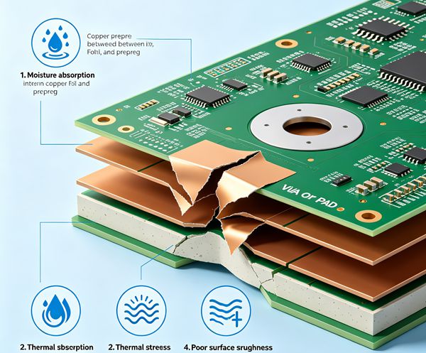
Table of Contents
What Is PCB Delamination?
PCB delamination refers to the separation of bonded layers within the circuit board structure.
Common locations include:
- Copper-to-laminate interfaces
- Prepreg-to-core interfaces
- Internal multilayer bonding surfaces
- Solder mask adhesion areas
Delamination may appear as:
- Blisters
- Air pockets
- Layer separation
- Surface swelling
- Internal voids
In severe cases, the board may become electrically unusable.
Related Reading: Multilayer PCB Manufacturing
Why PCB Delamination Is a Serious Reliability Problem
Unlike cosmetic defects, delamination directly affects the mechanical and electrical integrity of the PCB.
Potential consequences include:
- Open circuits
- Increased impedance variation
- Reduced insulation resistance
- Thermal failure
- Via reliability degradation
- Assembly defects
In automotive, industrial, and medical electronics, delamination often results in complete product failure.
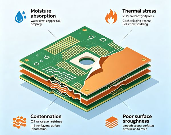
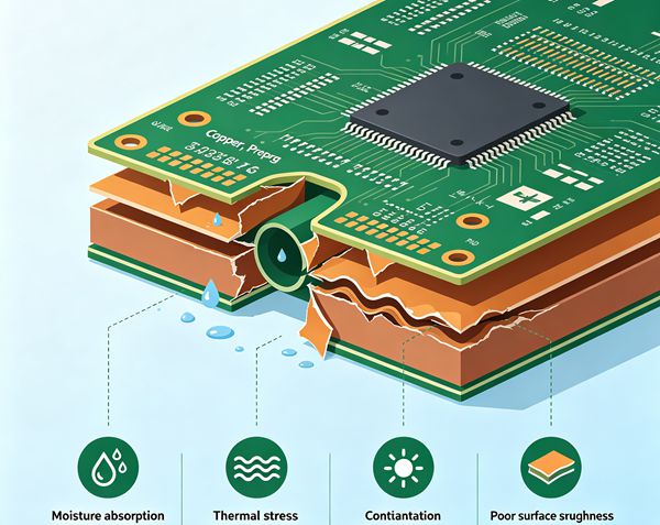
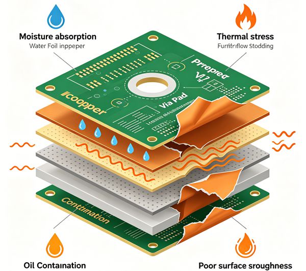
Common Causes of PCB Delamination
Excessive Moisture Absorption
Moisture is one of the most common causes of delamination.
PCB materials naturally absorb humidity during:
- Storage
- Transportation
- Production waiting periods
During reflow soldering, trapped moisture rapidly expands into steam.
This phenomenon is commonly called:
- Popcorning
- Steam-induced delamination
Pre-baking boards before assembly helps reduce this risk.
Internal Link: PCB Warpage and Reflow Deformation
Improper Lamination Parameters
The multilayer lamination process requires precise control of:
- Temperature
- Pressure
- Heating rate
- Cooling rate
Incorrect parameters can create weak bonding areas that eventually separate under thermal stress.
Common manufacturing issues include:
- Insufficient resin flow
- Uneven pressure distribution
- Incomplete curing
Poor Material Selection
Not all laminates perform equally under thermal stress.
Low-quality materials may exhibit:
- Poor peel strength
- High moisture absorption
- Reduced Tg performance
For demanding applications, engineers often specify:
- High Tg FR4
- Low-loss laminates
- Automotive-grade materials
Excessive Rework Cycles
Each rework cycle introduces additional thermal stress.
Repeated exposure to soldering temperatures may cause:
- Resin degradation
- Bond weakening
- Internal cracking
This issue is frequently observed in prototype builds and low-volume production runs.
Internal Link: Prototype PCB Manufacturing
Poor Copper Balance
Uneven copper distribution creates localized thermal expansion differences.
Consequences include:
- Internal stress accumulation
- Board deformation
- Delamination initiation
Proper stackup planning helps reduce these risks.
Internal Link: PCB Stackup Design Guide
How to Identify PCB Delamination
Visual Inspection
Early warning signs include:
- Surface bubbles
- White spots
- Blistering
- Lifted copper areas
Cross-Section Analysis
Cross-section testing reveals:
- Internal separation
- Resin voids
- Bonding defects
This method is commonly used during failure analysis.
X-Ray Inspection
For multilayer boards, X-ray analysis can help identify:
- Hidden voids
- Layer separation
- Structural abnormalities
Thermal Stress Testing
Reliability testing often includes:
- Thermal shock
- Thermal cycling
- Reflow simulation
These tests accelerate latent defects and reveal weak bonding structures.
How to Prevent PCB Delamination
Use High-Quality Materials
Material quality is the foundation of long-term reliability.
Important factors include:
- Glass transition temperature (Tg)
- Moisture resistance
- Peel strength
- Thermal expansion characteristics
Optimize Lamination Process Control
Manufacturers should monitor:
- Press temperature profiles
- Pressure consistency
- Resin flow behavior
- Cure conditions
Consistent lamination significantly improves bond strength.
Control Moisture Exposure
Recommended practices include:
- Vacuum packaging
- Dry storage conditions
- Moisture barrier bags
- Controlled floor life
Before assembly, baking may be required for moisture-sensitive boards.
Improve Stackup Design
A balanced stackup helps minimize internal stress.
Best practices include:
- Symmetrical layer structures
- Balanced copper distribution
- Controlled dielectric thickness
Internal Link: PCB Manufacturing Process
Reduce Excessive Rework
Each additional thermal cycle increases reliability risk.
Whenever possible:
- Verify designs thoroughly before production
- Minimize manual rework operations
- Use controlled repair procedures
Industries Most Affected by Delamination
Automotive Electronics
Thermal cycling and vibration accelerate failure mechanisms.
Industrial Equipment
Long operating hours create sustained thermal stress.
Power Electronics
High-current applications generate localized heating.
Related Reading: Power Electronics PCB Design for EV
Aerospace Systems
Extreme environmental conditions demand maximum structural integrity.
FAQ
A: The most common causes include moisture absorption, poor lamination control, low-quality materials, excessive thermal cycling, and improper stackup design.
A: Minor surface issues may sometimes be repaired, but internal delamination generally cannot be fully restored.
A: Visual inspection, cross-section analysis, X-ray inspection, and thermal stress testing are commonly used.
A: Yes. Lead-free processes typically operate at higher temperatures, increasing thermal stress on PCB materials.
A: High Tg laminates and low-moisture-absorption materials generally provide better resistance.
Conclusion
PCB delamination is a critical reliability concern that can affect electrical performance, mechanical stability, and product lifespan.
Most delamination failures can be prevented through:
- Proper material selection
- Controlled lamination processes
- Moisture management
- Balanced stackup design
- Effective quality control
By addressing these factors early in the design and manufacturing process, engineers can significantly improve PCB reliability and reduce long-term field failures.