A PCB stackup defines the arrangement of copper layers, prepregs, cores, and dielectric materials within a printed circuit board.
While often overlooked during early development, stackup design is one of the most important factors affecting:
- Signal integrity
- Controlled impedance
- EMI performance
- Power distribution
- Thermal behavior
- Manufacturing reliability
A well-designed stackup helps prevent costly redesigns and improves both electrical and mechanical performance.
Related Reading: PCB Manufacturing Process
Table of Contents
Why PCB Stackup Design Matters
Many PCB problems originate from poor layer planning rather than poor routing.
Common issues include:
- Impedance mismatch
- Excessive EMI
- Crosstalk
- Power instability
- PCB warpage
- Via reliability problems
A proper stackup establishes the foundation for successful PCB design.
Main Elements of a PCB Stackup
Copper Layers
Copper layers carry:
- Signals
- Power
- Ground references
Typical copper thicknesses include:
| Copper Weight | Thickness |
|---|---|
| 0.5 oz | 17 μm |
| 1 oz | 35 μm |
| 2 oz | 70 μm |
| 3 oz | 105 μm |
Higher copper weight improves current-carrying capability but affects impedance calculations.
Core Materials
The core provides structural support.
Functions include:
- Mechanical stability
- Dielectric separation
- Thermal performance
Material selection significantly affects signal quality.
Internal Link: High Frequency PCB Material Selection
Prepreg Layers
Prepreg acts as the bonding material between cores.
During lamination:
- Resin melts
- Layers bond together
- Final dielectric thickness is established
Prepreg characteristics directly influence impedance control.
Ground Planes
Ground planes provide:
- Return current paths
- Noise reduction
- EMI suppression
Continuous reference planes are essential for high-speed signals.
Power Planes
Power planes distribute current efficiently while reducing voltage fluctuations.
Benefits include:
- Lower impedance
- Improved power integrity
- Better thermal distribution
Common PCB Stackup Structures
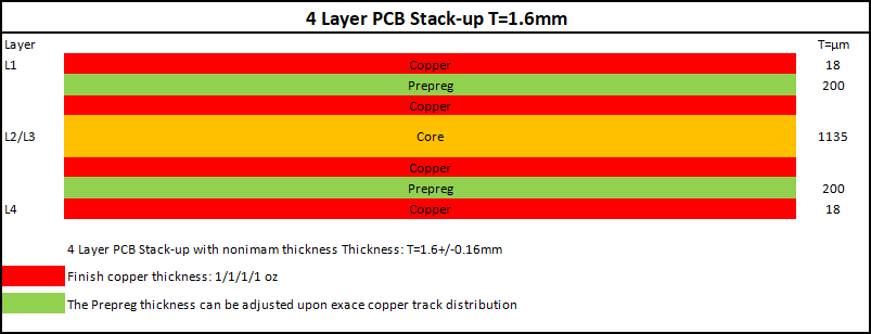
4-Layer PCB Stackup
A common arrangement is:
Signal
Ground
Power
Signal
Advantages:
- Cost-effective
- Good EMI control
- Suitable for many industrial products
Applications:
- Embedded systems
- Industrial controls
- Consumer electronics
Related Reading: 4 Layer PCB
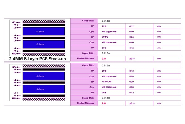
6-Layer PCB Stackup
Typical configuration:
Signal
Ground
Signal
Power
Ground
Signal
Benefits:
- Better signal isolation
- Improved impedance control
- Reduced EMI
Commonly used in:
- Communication equipment
- Industrial automation
- Networking products
8-Layer PCB Stackup
Typical arrangement:
Signal
Ground
Signal
Power
Ground
Signal
Ground
Signal
Advantages:
- Excellent signal integrity
- High routing density
- Reduced crosstalk
Applications:
- Servers
- High-speed communication
- Medical equipment
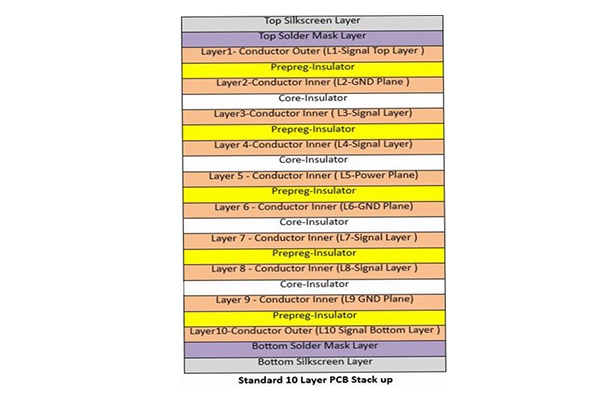
10-Layer and Above
Higher layer counts support:
- HDI routing
- Complex processors
- High-speed buses
- RF integration
Internal Link: Multilayer PCB Supplier
Stackup Design for Signal Integrity
Keep Signal Layers Adjacent to Ground Planes
This creates:
- Stable return paths
- Lower EMI
- Controlled impedance
Poor reference plane placement is one of the most common design mistakes.
Minimize Loop Area
Smaller current loops reduce:
- Radiation
- Noise
- Susceptibility to interference
Control Layer Transitions
Every via transition introduces:
- Discontinuities
- Reflection
- Potential signal degradation
Internal Link: PCB Via Failure Analysis
Stackup Design for Controlled Impedance
Controlled impedance depends on:
- Trace width
- Dielectric thickness
- Copper thickness
- Material Dk
Engineers should calculate impedance before routing begins.
Common targets include:
| Interface | Typical Impedance |
|---|---|
| USB | 90 Ω Differential |
| Ethernet | 100 Ω Differential |
| PCIe | 85 Ω Differential |
| DDR | 40–60 Ω Single Ended |
Stackup Design for EMI Reduction
EMI performance improves when:
Ground Planes Remain Continuous
Avoid:
- Large splits
- Plane interruptions
- Unnecessary cutouts
High-Speed Signals Stay Close to References
This minimizes:
- Radiation
- Crosstalk
- Signal loss
Power and Ground Layers Are Properly Coupled
Closely spaced planes create distributed capacitance.
Benefits include:
- Improved power integrity
- Reduced switching noise
Stackup Design for Manufacturability
Electrical performance alone is not enough.
The stackup must also be manufacturable.
Important considerations include:
Symmetrical Layer Structure
Balanced designs reduce:
- Warpage
- Internal stress
- Reliability failures
Internal Link: PCB Warpage and Reflow Deformation
Balanced Copper Distribution
Uneven copper can cause:
- Lamination stress
- Delamination
- Dimensional instability
Internal Link: PCB Delamination Causes and Prevention
Appropriate Dielectric Thickness
Avoid unnecessarily thin dielectric layers that increase manufacturing difficulty.
How to Design an Effective PCB Stackup
- Step 1
Define:
. Signal speed
. Layer count
. Power requirements - Step 2
Select suitable materials based on:
. Frequency
. Thermal requirements
. Reliability targets
Related Reading: High Frequency PCB Material Selection - Step 3
Allocate dedicated ground planes early.
- Step 4
Determine impedance requirements before routing.
- Step 5
Review manufacturability with your PCB fabrication partner.
- Step 6
Verify performance using simulation tools.
Common PCB Stackup Mistakes
Routing Without Stackup Planning
Often leads to impedance problems.
Insufficient Ground Layers
Results in:
- EMI issues
- Poor signal integrity
Asymmetrical Structures
Increase warpage risk.
Excessive Layer Changes
Create unnecessary signal discontinuities.
Ignoring Material Properties
Can produce unreliable impedance performance.
FAQ
A: The required layer count depends on routing density, signal speed, and power distribution requirements.
A: Stackup affects signal integrity, EMI, manufacturability, and reliability.
A: No. Accurate impedance calculations require a defined stackup structure.
A: Generally, signal layers should be adjacent to continuous reference planes.
A: Before PCB layout starts. Early stackup planning prevents costly redesigns later.
Conclusion
PCB stackup design is one of the most important decisions in PCB development.
A properly engineered stackup improves:
- Signal integrity
- Impedance control
- EMI performance
- Reliability
- Manufacturability
By combining sound electrical design principles with manufacturing considerations, engineers can create PCB designs that perform reliably from prototype through mass production.