A 6 layer PCB offers a balance between electrical performance, routing capability, and manufacturing cost. Compared with 4-layer boards, six-layer structures provide additional routing space, better signal isolation, and improved power integrity, making them suitable for increasingly complex electronic products.
6 layer PCBs are commonly used in:
- Industrial automation
- Communication equipment
- Automotive electronics
- Embedded control systems
- Networking products
- Medical devices
TOPFAST provides custom 6 layer PCB manufacturing with support for controlled impedance, multilayer stackups, and prototype to volume production.
Table of Contents
Why Choose a 6 Layer PCB?
Compared with two-layer and four-layer boards, six-layer PCBs offer several advantages.
Improved Signal Integrity
Additional reference planes reduce:
- Crosstalk
- Signal reflection
- EMI emissions
This makes 6 layer boards suitable for high-speed digital applications.
Related Reading: PCB Stackup Design Guide
Higher Routing Density
Two additional layers provide:
- More signal routing channels
- Easier component placement
- Reduced board size
This helps designers accommodate increasingly complex circuits.
Better Power Distribution
Dedicated power and ground planes improve:
- Voltage stability
- Noise suppression
- Return current paths
Enhanced Reliability
Balanced multilayer structures help reduce:
- Warpage
- Mechanical stress
- Thermal deformation
Internal Link: PCB Warpage and Reflow Deformation
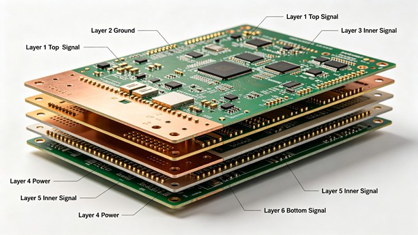
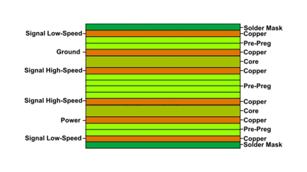
Typical 6 Layer PCB Stackup
One of the most common stackup configurations is:
Layer 1  Signal
Layer 2  Ground
Layer 3  Signal
Layer 4  Power
Layer 5  Ground
Layer 6  Signal
Advantages include:
- Stable impedance control
- Improved EMI suppression
- Better signal return paths
- Reduced noise coupling
Other stackup arrangements may be optimized according to:
- High-speed signals
- RF circuits
- Power electronics
- HDI designs
Related Reading: High Frequency PCB Material Selection
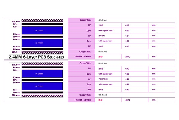
Standard Specifications
| Parameter | Capability |
|---|---|
| Layer Count | 6 Layers |
| Material | FR4, High Tg, Rogers |
| Copper Weight | 0.5–3 oz |
| Board Thickness | 0.4–3.2 mm |
| Min Trace/Space | 3/3 mil |
| Min Drill Size | 0.15 mm |
| Surface Finish | HASL, ENIG, OSP |
| Solder Mask Color | Green, Blue, Black, White, Red |
| Impedance Control | Available |
| IPC Standard | IPC Class 2 / Class 3 |
Materials Available for 6 Layer PCBs
Standard FR4
Suitable for:
- Industrial electronics
- Consumer products
- Embedded systems
Benefits:
- Low cost
- Good mechanical strength
- Wide availability
High Tg Materials
Recommended for:
- Automotive electronics
- Lead-free assembly
- High-temperature environments
Higher Tg materials provide better thermal stability and reliability.
Rogers Materials
Suitable for:
- RF circuits
- Microwave systems
- High-speed communication
Internal Link: High Frequency PCB Material Selection
6 Layer PCB Applications
Industrial Control Systems
Industrial products often require:
- Long service life
- High reliability
- Stable signal transmission
Communication Equipment
Routers, gateways, and switches commonly use 6 layer boards to support:
- Differential pair routing
- Controlled impedance
- EMI reduction
Automotive Electronics
Applications include:
- ECU modules
- Battery management systems
- ADAS controllers
Related Reading: Automotive PCBA Reliability Design
Medical Devices
Medical electronics require:
- Stable performance
- High manufacturing quality
- Long-term reliability
Power Electronics
Motor drives and power converters benefit from:
- Better thermal management
- Improved current distribution
Internal Link: Power Electronics PCB Design for EV
Design Considerations for 6 Layer PCBs
Stackup Planning
Proper stackup design improves:
- Signal integrity
- Power integrity
- Manufacturability
Related Reading: PCB Stackup Design Guide
Controlled Impedance
Many 6 layer designs require impedance-controlled traces.
Common impedance values include:
- 50 Ω single-ended
- 90 Ω differential (USB)
- 100 Ω differential (Ethernet)
Via Reliability
Via quality becomes increasingly important in multilayer structures.
Designers should consider:
- Aspect ratio
- Copper thickness
- Thermal expansion
Related Reading: PCB Via Failure Analysis
Copper Balance
Balanced copper distribution helps prevent:
- Bow and twist
- Internal stress
- Delamination
Internal Link: PCB Delamination Causes and Prevention
How to Order a Custom 6 Layer PCB
- Step 1
Provide:
. Gerber files
. Drill files
. Stackup requirements - Step 2
Confirm:
. Material type
. Copper thickness
. Surface finish - Step 3
Review engineering feedback and DFM recommendations.
- Step 4
Prototype verification before mass production.
- Step 5
Proceed to full production.
Need a Custom 6 Layer PCB?
TOPFAST supports:
✓ Standard and high Tg materials
✓ Controlled impedance
✓ Prototype and volume production
✓ IPC Class 2 and Class 3 manufacturing
✓ Engineering review and DFM support
Frequently Asked Questions
A: 6 layer PCBs are commonly used in communication equipment, automotive electronics, industrial control systems, and medical devices.
A: Common thicknesses include:
. 1.0 mm
. 1.2 mm
. 1.6 mm
. 2.0 mm
Custom thicknesses are also available.
A: For higher routing density and better signal integrity, a 6 layer PCB generally offers superior performance.
A: Yes. Six-layer structures are widely used for controlled impedance applications.
A: FR4 is suitable for most applications, while high Tg and Rogers materials are preferred for demanding environments and RF designs.
Conclusion
A 6 layer PCB provides an effective balance between cost, routing density, signal integrity, and reliability.
With additional signal and reference layers, six-layer boards support increasingly complex electronic systems while maintaining stable performance and manufacturability.
Through optimized stackup design, appropriate material selection, and controlled manufacturing processes, 6 layer PCBs can deliver reliable performance from prototype development to high-volume production.