Table of Contents
PCB Design
PCB (Printed Circuit Board) production begins with the precision design phase. Professional design engineers utilize advanced Electronic Design Automation (EDA) tools to meticulously create circuit schematics and PCB layouts based on functional requirements. This critical step not only determines the circuit’s logical relationships but also precisely plans:
- Optimal component placement
- Efficient trace routing design
- Signal integrity assurance
- Electromagnetic compatibility optimization
After design completion, the circuit diagrams and PCB layouts are converted into industry-standard Gerber file format, providing precise guidance for subsequent production processes. Modern PCB design also fully considers Design for Manufacturability (DFM) and Design for Testing (DFT) principles to ensure a smooth transition from design to mass production.
Material Selection
High-quality raw materials form the foundation of superior PCB manufacturing. Key materials include:
| Material Type | Typical Examples | Key Quality Indicators |
|---|---|---|
| Substrate Materials | FR-4, High-frequency Materials | Dielectric Constant, CTE |
| Conductive Layer | Electrolytic Copper Foil | Thickness Uniformity, Surface Roughness |
| Solder Mask | Liquid Photoimageable Ink | Heat Resistance, Insulation Properties |
| Surface Treatment | ENIG, OSP | Solderability, Oxidation Resistance |
All materials must pass rigorous Incoming Inspection (MI), including:
- Dimensional accuracy measurements
- Physical property testing
- Chemical compatibility verification
- Environmental reliability assessment
The cleaning process for substrate materials is particularly critical, utilizing cleanroom environments and precision cleaning equipment to achieve nanoscale surface cleanliness standards.
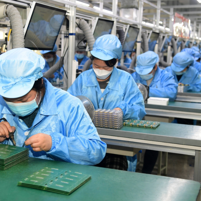
Inner Layer Circuit Production: Birth of Precision Patterns
Inner layer fabrication represents the core process of multilayer PCB production, with key manufacturing steps including:
- Substrate Pre-treatment:
- Precision cutting to production size
- Chemical cleaning to remove surface contaminants
- Surface roughening to enhance adhesion
- Pattern Transfer:
- Dry film lamination using high-precision coating machines
- UV exposure employing LDI (Laser Direct Imaging) technology
- Precision development with ±1°C temperature and ±0.5% concentration control
- Etching Formation:
- Acid or alkaline etching process selection
- Line width control accuracy of ±0.02mm
- 100% Automated Optical Inspection (AOI)
Process parameter control at this stage directly impacts the final product
- Signal transmission quality
- Current carrying capacity
- Long-term reliability performance
Multilayer Lamination and Precision Drilling Technology
For High-Density Interconnect (HDI) PCBs, multilayer lamination is a key manufacturing technology:
Lamination Process Flow:
- Brown Oxide Treatment: Enhances interlayer bonding
- Layup Alignment: Utilizes X-ray alignment systems
- Hot Press Lamination: Precisely controlled temperature profiles
- Post-processing: Routing, edge grinding, etc.
Drilling Technology Advancements:
- Mechanical Drilling: Minimum hole diameter 0.15mm
- Laser Drilling: Microvia diameter down to 0.05mm
- Depth Control: ±0.025mm accuracy
Modern PCB factories employ intelligent drilling systems featuring:
- Automatic tool changing
- Real-time drill bit wear monitoring
- Adaptive drilling parameter adjustment
Outer Layer Circuits and Surface Treatment Processes
Outer layer patterning adopts modified Semi-Additive Process (mSAP) technology, offering advantages including:
- Finer circuit production capability
- Higher aspect ratio control
- Superior surface planarity
Solder Mask Process Key Points:
- Ink thickness control: 20-25μm
- Curing temperature profile optimization
- Opening accuracy ±0.05mm
Surface Treatment Selection Guide:
| Process Type | Application Scenario | Characteristics |
|---|---|---|
| ENIG | High-reliability products | Excellent solderability and oxidation resistance |
| HASL | Consumer electronics | Cost-effective |
| OSP | Short-term storage products | Environmentally friendly |
| Gold Plating | High-frequency products | Superior signal integrity |
Comprehensive Quality Assurance System
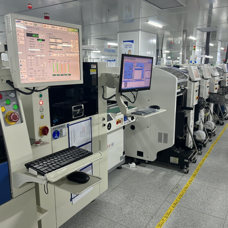
Modern PCB manufacturing employs multi-level inspection systems:
- Process Control:
- First Article Inspection (FAI)
- Statistical Process Control (SPC)
- Real-time monitoring systems
- Finished Product Inspection:
- AOI Automated Optical Inspection
- Flying Probe/Test Fixture
- Impedance Testing (TDR)
- Microsection Analysis
- Reliability Testing:
- Thermal cycling tests
- Humidity aging tests
- Mechanical stress tests
Innovation Trends in PCB Technology
- High-Density Interconnect (HDI) Technology:
- Any-layer interconnection design
- Finer line width/spacing
- Embedded component technology
- Flexible Electronics:
- Bendable circuit boards
- Wearable device applications
- 3D circuitry
- Green Manufacturing:
- Halogen-free materials
- Wastewater recycling systems
- Energy-efficient production processes
Industry Applications and Market Outlook
PCB technology has penetrated virtually all electronic sectors:
- 5G Communications: Surging demand for high-frequency PCBs
- Automotive Electronics: Autonomous driving boosting HDI applications
- Medical Devices: High-reliability specialty substrates
- Consumer Electronics: Thinner and smaller form factors
According to Primark forecasts, the global PCB market will reach $89.2 billion by 2025, with a CAGR of approximately 4.3%. IC substrates and high-layer count boards will become the fastest-growing segments.
Through continuous process optimization and intelligent production systems, the PCB industry is rapidly advancing toward higher precision, greater reliability, and enhanced environmental sustainability, providing solid foundational support for electronics innovation.