Hohe Dichte Unterhaltungselektronik PCB Lösungen
Die nächste Generation smarter Geräte. Präzisions-HDI- und Rigid-Flex-Lösungen für Smartphones, Wearables und IoT-Ökosysteme.
Sofortangebot anfordern
0%
Hervorragende Erträge
0+
Jahre Berufserfahrung
0h
Schnelles Prototyping
Warum sollten Sie sich bei Unterhaltungselektronik für TOPFAST entscheiden?
Innovation durch Miniaturisierung, hohe Geschwindigkeit und kostengünstige Massenproduktion vorantreiben.
Kompetenz in der Miniaturisierung
Branchenführende HDI-Technologie mit Microvias auf jeder Schicht, um komplexe Schaltungen in schlanke, kompakte Gehäuse zu integrieren.
Kosten-Leistungs-Optimierung
Optimierte Fertigungsprozesse, die darauf ausgelegt sind, Produkte von höchster Qualität zu wettbewerbsfähigen Marktpreisen zu liefern.
Agile Lieferkette
Skalierbare Produktionskapazitäten, die sich von der schnellen Prototypenerstellung bis hin zur Massenproduktion erstrecken, um saisonalen Anforderungen gerecht zu werden.
Sofortiges Angebot anfordern
✓ ISO 9001 & UL Certified Production
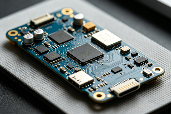
Technische Kompetenzen der Verbraucher
Unterstützung von leistungsstarken Handheld-Geräten und Smart-Home-Geräten durch hochdichte Verbindungen.
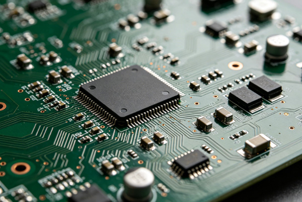
Mobilgeräte und Handheld-Geräte
Spezialisiert auf HDI-Leiterplatten mit beliebiger Schichtenanzahl und dünne Substrate für Smartphones, Tablets und Spielkonsolen.
Any-Layer / ELIC
2 Meilen / 2 Meilen
Nur 0,2 mm dünn
ENIG / OSP
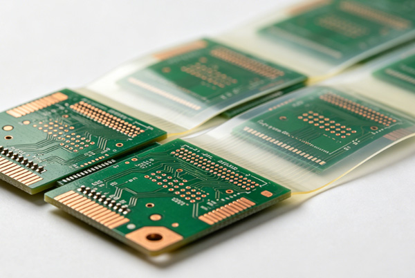
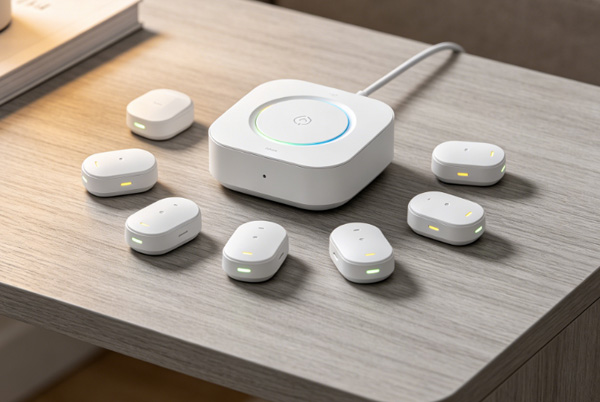
Intelligente Wearables & IoT
Flexible und Rigid-Flex-Leiterplatten, die für gebogene Formfaktoren und eine langlebige Integration in rund um die Uhr tragbare Geräte entwickelt wurden.
Starr-flexible Mehrschichtplatine
SMT mit hoher Packungsdichte
Lasergebohrt
Auf Polyimid (PI)-Basis
Partner im Bereich Verbrauchertechnologie
„Ihre Fähigkeit, HDI-Leiterplatten mit beliebig vielen Schichten für unser Flaggschiff-Smartphone zu fertigen, war beeindruckend. Die Signalintegrität ist selbst bei hohen Geschwindigkeiten hervorragend.“
„Dank des Rigid-Flex-Designs, das sie für unsere neueste Smartwatch entwickelt haben, konnten wir die Dicke des Geräts um 15 % reduzieren. Sehr zu empfehlen.“
„Dank des schnellen Prototyping konnten wir unseren Zeitplan für die Produkteinführung einhalten. Durch ihr DFM-Feedback haben wir zwei Wochen an Konstruktionsänderungen eingespart.“
„Konsistenz in der Massenproduktion ist für uns entscheidend. Mit Topfast haben wir unsere Produktion von 1.000 auf 100.000 Einheiten gesteigert, ohne dass die Qualität darunter gelitten hat.“
„Hochwertige Verarbeitung und 100-prozentige Prüfung. Seit wir auf Topfast umgestiegen sind, ist die DOA-Rate bei unseren Consumer-Tablets deutlich gesunken.“
„Professionelle Kommunikation und hervorragender technischer Support bei der Umstellung auf halogenfreie Materialien. Ideal für unsere Umweltinitiativen.“
Spezifikationen und Normen für Leiterplatten für Verbraucherprodukte
| Parameter | Standardverbraucher | High-End-Gerät (HDI) |
|---|---|---|
| Grundmaterial | FR4 (Standard) | Halogenfrei, BT-Harz, PI |
| Kupferdicke | Eine halbe Unze – eine Unze | Bis zu 85 g (Schnellladung) |
| Oberflächenbehandlung | OSP / ENIG | ENEPIG / Zinnbad |
| Min. Spurweite/Abstand | 3 / 3 Meilen | 1,5 / 1,5 mil (feiner Rasterabstand) |
| Validierung | CE / FCC / RoHS | EMI-Abschirmung / Hochgeschwindigkeits-Signalübertragung |
| Qualitätskontrolle | IPC-Klasse 2 | Unterstützung für die Schutzklassen IP2 und IP3 |
Agiler Fertigungsworkflow
1
Feedback zum Design
Sofortige DFM-Analyse zur Optimierung für eine ertragreiche, kompakte Serienfertigung.
2
Präzisions-HDI
Laserdirektbelichtung und Microvia-Bohren für modernste Mobilfunk-Schaltkreise.
3
Signalintegrität
Fortschrittliche Impedanzprüfungen zur Gewährleistung einer einwandfreien 5G- und WLAN-Konnektivität.
4
Abschließende Inspektion
100 % AOI- und elektrische Prüfungen, um die Zuverlässigkeit im Einsatz beim Endverbraucher zu gewährleisten.
Anwendungen im Alltag
Häufig gestellte Fragen zu Leiterplatten für Endverbraucher
Wie schnell können Sie Prototypen für Endverbraucher liefern?
Wir bieten einen 24-Stunden-Schnellprototyping-Service für standardmäßige 2-Lagen-Leiterplatten sowie eine Lieferzeit von 2 bis 4 Tagen für komplexe mehrschichtige HDI-Designs, damit Sie Ihre Entwicklung beschleunigen können.
Unterstützen Sie Any-Layer-HDI für ultraschlanke Geräte?
Ja. Wir sind auf die ELIC-Technologie (Every Layer Interconnect) spezialisiert, die eine maximale Schaltungsdichte in schlanken Smartphones und tragbaren Elektronikgeräten ermöglicht.
Können Sie bei Produkteinführungen große Produktionsmengen bewältigen?
Auf jeden Fall. Unsere Anlagen sind auf Skalierbarkeit ausgelegt und decken den gesamten Prozess ab – von der Einführung neuer Produkte (NPI) bis hin zur Massenproduktion in großen Stückzahlen bei gleichbleibender Qualität.
Sind Ihre Materialien RoHS- und REACH-konform?
Ja, alle unsere Standardmaterialien und Oberflächenbeschichtungen für Unterhaltungselektronik entsprechen vollständig den Umweltvorschriften von RoHS und REACH.