Hochpräzise Halbleiter-Leiterplatte Lösungen
Wir erweitern die Grenzen der Mikroelektronik. Wir bieten Leiterplattenlösungen mit extrem hoher Schichtenanzahl und feinem Raster für IC-Tests, Prüfkarten und Anwendungen auf Substratebene.
Technisches Angebot anfordern
0+
Anzahl der Schichten
0mm
Min. Abstandshalter
0%
Auf Mikroschnitt geprüft
Warum Sie sich bei Halbleitern für TOPFAST entscheiden sollten
Technische Spitzenleistungen für die komplexesten Siliziumarchitekturen der Welt.
Extrem hohe Schichtdichte
Spezialisiert auf die Herstellung dicker Leiterplatten mit hoher Lagenanzahl (bis zu 8,0 mm Dicke) für komplexe Load Boards und Prüfkarten.
Experten für Wärmemanagement
Einsatz modernster Kupfermünztechnologie und Laminate mit hoher Wärmeleitfähigkeit für Hochleistungs-Einbrennprüfumgebungen.
Registrierung mit Nanopräzision
Durch den Einsatz hochwertiger LDI-Systeme und spezieller Ausrichtungsverfahren wird eine perfekte Passgenauigkeit über Dutzende von Signalschichten hinweg gewährleistet.
Sofortangebot für Ingenieurdienstleistungen
✓ Support for ENEPIG & Hard Gold
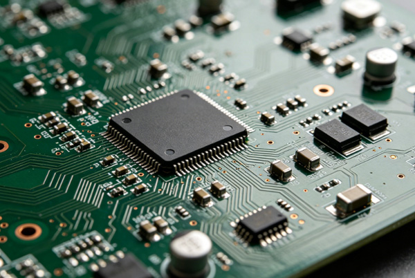
Fähigkeiten im Bereich Halbleiterqualität
Präzisionsfertigungsstandards, die für Null-Toleranz-Prüfungen und Substratanwendungen optimiert sind.
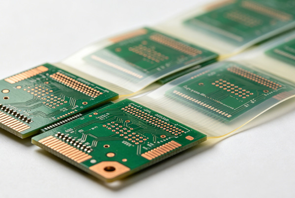
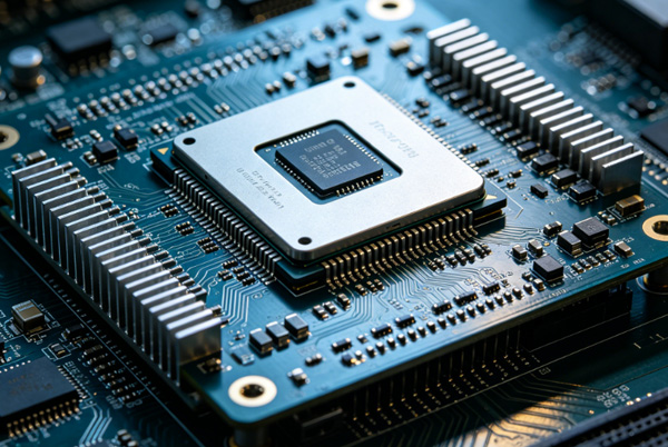
IC-Testschnittstellenkarten
Spezialfertigung von Lastplatinen und DUT-Platinen (Device Under Test) mit extrem ebener Oberflächenbeschaffenheit und BGA-Pads mit feinem Rastermaß.
Bis zu 20:1
min. 0,3 mm
Bis zu 8,0 mm
Planar ENEPIG
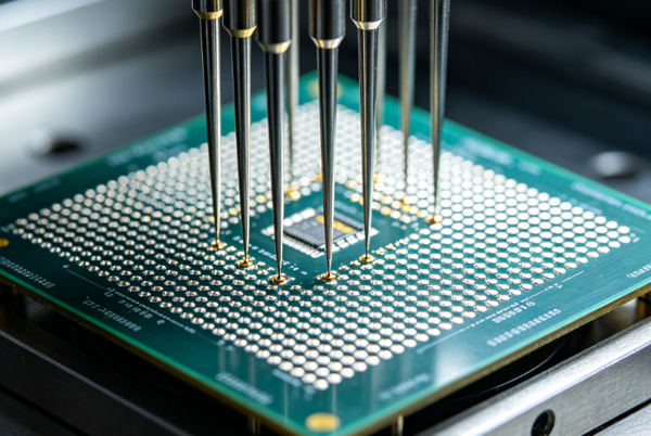
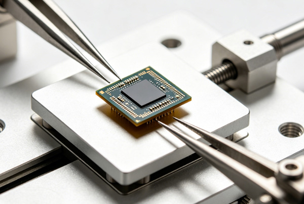
Hochentwickelte Prüfkarten
Lieferung der Kernkomponenten für Tests auf Wafer-Ebene mit hochdichten vertikalen Verbindungen und hervorragender mechanischer Stabilität.
Geringe Übertragungsverzögerung
Hybrid-Aufbau
Steuerung der Rückbohrung
PTFE mit extrem geringen Verlusten
Branchenverband
Unterstützung der Lieferkette von Fabless-Designhäusern bis hin zu globalen Testzentren.
„Topfast ist einer der wenigen Anbieter, der Leiterplatten mit mehr als 40 Schichten liefern kann, die die für unsere GPU-Tests erforderliche Passgenauigkeit aufweisen.“
„Die Qualität der ENEPIG-Oberfläche und die Ebenheit der Kontaktflächen sind ideal für die Montage unserer BGA-Sockel mit hoher Pin-Anzahl.“
„Ihre technische Beratung bei der Entwicklung unserer Hochleistungs-Einbrennplatine hat uns vor einem schwerwiegenden thermischen Ausfall bewahrt.“
„Unübertroffene Lieferzeiten für mehrschichtige Prototypen. Sie wissen, wie dringend die Freigabezyklen in der Halbleiterindustrie sind.“
„Ihre Kompetenz bei der Durchführung von Back-Drilling mit hohem Seitenverhältnis ist für unsere Anforderungen an die Signalintegrität bei hohen Geschwindigkeiten von entscheidender Bedeutung.“
Spezifikationen für Halbleiter-Leiterplatten
Extreme Fertigungsparameter, die speziell auf die Prüfung und Zuverlässigkeit von integrierten Schaltkreisen zugeschnitten sind.
| Parameter | Hochleistungsfähigkeit | Option für höchste Präzision |
|---|---|---|
| Maximale Anzahl von Ebenen | 32–40 Schichten | Bis zu 64 Ebenen |
| Min. Linienbreite / Abstand | 2,5 Meilen / 2,5 Meilen | 1,8 Meilen / 1,8 Meilen (SLP) |
| Bohrungs-Seitenverhältnis | 12:1 | 20:1 (extrem dicke Platten) |
| Planarität der Oberfläche | < 5µm Tolerance | < 2µm (Laser Leveling) |
| Materialgruppen | FR4 mit hohem Glasübergangstemperaturbereich, Megtron 6/7 | Tachyon 100G, Isola Terra |
| Oberfläche | ENIG / Hartgold | ENEPIG / Selektives Gold |
Unser Fertigungsprozess für IC-Qualität
Ein mehrstufiger, hochauflösender Prozess, der eine fehlerfreie Schnittstellenhardware gewährleistet.
1
SI/PI-Validierung
Gründliche Simulation der Signal- und Stromversorgungsintegrität, um sicherzustellen, dass das Design hochfrequente IC-Lasten bewältigen kann.
2
Laserfabrik
Laserbohren und -abbildung im Submikronbereich zur Herstellung ultrafeiner Verbindungen für Sondenkartensubstrate.
3
Vertikale Steuerung
Spezielle Verkupferungsverfahren zur Gewährleistung einer gleichmäßigen Impedanz bei Durchkontaktierungen mit hohem Seitenverhältnis.
4
Abschließende Analyse
Automatisierte 3D-AOI und 100-prozentige Mikroschnittanalyse zur Überprüfung der internen Passgenauigkeit und der thermischen Stabilität.
Treiber der Innovation in der Halbleiterbranche
Unsere Leiterplatten bilden die Grundlage für die Prüfung und Validierung von Computerhardware der nächsten Generation.

Häufig gestellte Fragen zu Halbleiter-Leiterplatten
Einblicke in die Fertigung von Leiterplatten mit hoher Schichtenanzahl und in Präzisionsprüfgeräte.
Wie gewährleistet man die Passgenauigkeit bei Leiterplatten mit mehr als 40 Schichten?
Wir setzen modernste Mass-Lam-Systeme mit Röntgenbohrverfahren und LDI-Bildgebung ein. Unsere Umgebungsbedingungen werden streng nach den Reinraumstandards der ISO-Klasse 5 für diese Schichten eingehalten, um thermische Ausdehnungsunterschiede oder Staubverunreinigungen während des Laminierungsprozesses zu vermeiden.
Können Sie extrem dickes Kupfer für Hochleistungs-Einbrennplatinen verarbeiten?
Ja, wir unterstützen dickes Kupfer mit einer Dicke von bis zu 10 oz für Stromverteilungsschichten. Außerdem integrieren wir Kupferplättchen und Kühlkörper direkt in die Leiterplattenstruktur, um die extremen thermischen Belastungen bei Hochleistungs-Chiptests zu bewältigen.
Wie gut sind Sie in der Lage, die Signalintegrität bei hohen Geschwindigkeiten zu gewährleisten?
Wir bieten fortschrittliches Rückbohren zur Beseitigung von Via-Stubs an und arbeiten mit einer breiten Palette von Materialien mit niedrigem DK/DF-Wert, wie beispielsweise Panasonic Megtron 7 und Isola Tachyon. Wir stellen sicher, dass die Signalausbreitung über die gesamte Schnittstelle der Testplatine hinweg bei Geschwindigkeiten von bis zu 112 Gbit/s konsistent bleibt.
Bieten Sie Mikroschnittanalysen für Produkte in Halbleiterqualität an?
Standard. Jeder Auftrag für Halbleiter-Leiterplatten umfasst einen detaillierten Mikroschnittbericht, die Ergebnisse der thermischen Belastungsprüfung sowie eine vollständige Analyse der ionischen Verunreinigungen als Teil unserer Lieferdokumentation (CoC).