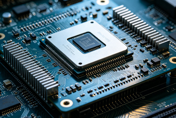
عالية الدقة لوحة دوائر مطبوعة لأشباه الموصلات الحلول
تخطي حدود الإلكترونيات الدقيقة. نقدم حلولاً للوحات الدوائر المطبوعة (PCB) ذات عدد طبقات فائق ودقة عالية، مخصصة لاختبار الدوائر المتكاملة وبطاقات الاختبار والتطبيقات على مستوى الركيزة.
اطلب عرض أسعار فني
0+
القدرة على حساب عدد الطبقات
0mm
الحد الأدنى لدعم المسافة بين الأعمدة
0%
تم اختبار المقطع المجهري
لماذا تختار TOPFAST في مجال أشباه الموصلات
التميز الهندسي لأكثر بنى السيليكون تعقيدًا في العالم.
كثافة طبقات فائقة
متخصصون في تصنيع الألواح السميكة ذات الطبقات المتعددة (بسماكة تصل إلى 8.0 مم) المستخدمة في لوحات التحميل المعقدة وبطاقات الاختبار.
خبراء إدارة الحرارة
التعامل مع التكنولوجيا المتطورة للعملات النحاسية والرقائق ذات الموصلية الحرارية العالية في بيئات اختبار التحمل عالية الطاقة.
التسجيل بدقة نانوية
الاستعانة بأنظمة LDI المتطورة وتقنيات محاذاة متخصصة لضمان التوافق التام بين عشرات طبقات الإشارات.
عرض أسعار فوري لخدمات الهندسة
✓ Support for ENEPIG & Hard Gold
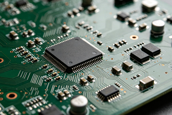
قدرات على مستوى صناعة أشباه الموصلات
معايير تصنيع دقيقة مُحسَّنة خصيصًا لاختبارات عدم التسامح مطلقًا وتطبيقات الركائز.
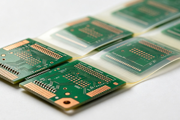
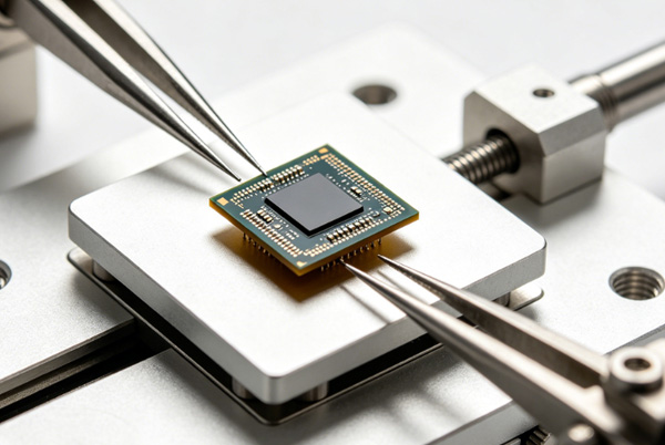
لوحات واجهة اختبار الدوائر المتكاملة
تصنيع متخصص للوحات التحميل ولوحات الأجهزة قيد الاختبار (DUT) ذات الأسطح المسطحة للغاية ووسادات BGA ذات المسافات الدقيقة.
تصل إلى 20:1
0.3 مم على الأقل
حتى 8.0 مم
بلانار ENEPIG
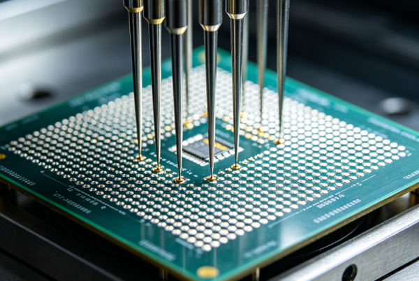
بطاقات الاختبار المتطورة
توفير الأجهزة الأساسية لاختبار الرقائق باستخدام وصلات رأسية عالية الكثافة واستقرار ميكانيكي فائق.
تأخير منخفض في الانتشار
البناء الهجين
التحكم في الحفر الخلفي
PTFE ذو خسارة منخفضة للغاية
صندوق الصناعة
دعم سلسلة التوريد بدءًا من شركات التصميم التي لا تمتلك مصانع إنتاج وصولاً إلى مراكز الاختبار العالمية.
"تُعد Topfast واحدة من الشركات القليلة القادرة على توفير لوحات تحميل ذات أكثر من 40 طبقة بدقة التسجيل التي تتطلبها اختبارات وحدات معالجة الرسومات (GPU) الخاصة بنا."
"تتميز تشطيبات ENEPIG وتسطيح الوسادات التي تنتجها الشركة بجودة مثالية لتركيب مآخذ BGA ذات عدد المسامير الكبير التي نستخدمها."
"لقد أنقذتنا استشاراتهم الفنية أثناء تصميمنا للوحة الاختبار عالية الطاقة من حدوث عطل حراري خطير."
"مدة إنجاز لا تضاهى للنماذج الأولية متعددة الطبقات. إنهم يدركون مدى إلحاح دورات إصدار أشباه الموصلات."
"إن قدرتها على التعامل مع عمليات الحفر الخلفي ذات النسبة الطولية العالية أمر ضروري لتلبية احتياجاتنا المتعلقة بسلامة الإشارات عالية السرعة."
مواصفات لوحات الدوائر المطبوعة لأشباه الموصلات
معايير تصنيع متطرفة مصممة خصيصًا لاختبار الدوائر المتكاملة وضمان موثوقيتها.
| المعلمة | قدرات عالية المواصفات | خيار الدقة الفائقة |
|---|---|---|
| الحد الأقصى لعدد الطبقات | 32 - 40 طبقة | ما يصل إلى 64 طبقة |
| الحد الأدنى لعرض الخط / التباعد | 2.5 ميل / 2.5 ميل | 1.8 ميل / 1.8 ميل (مستوى سطح البحر) |
| نسبة العرض إلى الارتفاع في الحفر | 12:1 | 20:1 (ألواح فائقة السُمك) |
| استواء السطح | < 5µm Tolerance | < 2µm (Laser Leveling) |
| مجموعات المواد | FR4 عالي درجة حرارة الانصهار، Megtron 6/7 | تاشيون 100G، إيزولا تيرا |
| تشطيب السطح | ENIG / الذهب الصلب | ENEPIG / الذهب الانتقائي |
مسار التصنيع الخاص بنا للمنتجات ذات الجودة الصناعية
عملية متعددة المراحل وعالية الدقة تضمن خلو الأجهزة الطرفية من أي عيوب.
1
التحقق من صحة SI/PI
محاكاة دقيقة لسلامة الإشارة والطاقة لضمان قدرة التصميم على التعامل مع أحمال الدوائر المتكاملة عالية التردد.
2
ليزر فاب
الحفر والتصوير بالليزر بدقة أقل من الميكرون لإنشاء وصلات داخلية فائقة الدقة لركائز بطاقات الاختبار.
3
التحكم الرأسي
عمليات طلاء بالنحاس متخصصة لضمان ثبات المعاوقة عبر الثقوب ذات النسبة الطولية العالية.
4
التحليل النهائي
التفتيش البصري الآلي ثلاثي الأبعاد (AOI) والتحليل الكامل للمقاطع المجهرية للتحقق من التوافق الداخلي والاستقرار الحراري.
دفع عجلة الابتكار في مجال السيليكون
تُستخدم لوحات الدوائر المطبوعة الخاصة بنا في إجراء الاختبارات والتحقق من صحة أجهزة الحوسبة من الجيل التالي.

الأسئلة الشائعة حول لوحات الدوائر المطبوعة لأشباه الموصلات
نظرة متعمقة على تصنيع الدوائر ذات عدد الطبقات الكبير وأجهزة الاختبار الدقيقة.
كيف يمكن الحفاظ على دقة التسجيل في اللوحات التي تحتوي على أكثر من 40 طبقة؟
نحن نستخدم أحدث أنظمة Mass Lam المزودة بتقنية الحفر بالأشعة السينية والتصوير LDI. كما نحافظ بدقة على ضوابطنا البيئية وفقًا لمعايير غرف الأبحاث النظيفة من الفئة 5 وفقًا لمعايير ISO، وذلك لضمان عدم حدوث أي تباين في التمدد الحراري أو تلوث بالغبار خلال دورة التصفيح.
هل يمكنكم التعامل مع النحاس شديد السُمك المستخدم في لوحات الاختبار عالية الطاقة؟
نعم، نحن ندعم استخدام النحاس الثقيل الذي يصل وزنه إلى 10 أونصات في طبقات توزيع الطاقة. كما نقوم بدمج قطع نحاسية ومبددات حرارية مباشرةً في هيكل لوحة الدوائر المطبوعة (PCB) للتعامل مع الأحمال الحرارية الشديدة أثناء اختبار الرقائق في ظروف الضغط الشديد.
ما هي قدراتكم في مجال سلامة الإشارات عالية السرعة؟
نقدم خدمة الحفر الخلفي المتطورة للتخلص من بقايا الثقوب، ونعمل مع مجموعة واسعة من المواد ذات المعاملات العازلة (DK/DF) المنخفضة مثل Panasonic Megtron 7 وIsola Tachyon. ونضمن استمرار انتشار الإشارة بشكل متسق عبر واجهة لوحة الاختبار بأكملها بسرعات تصل إلى 112 جيجابت في الثانية.
هل تقدمون خدمة تحليل المقاطع المجهرية للمنتجات المخصصة لصناعة أشباه الموصلات؟
قياسي. تتضمن كل طلبية لوحات الدوائر المطبوعة شبه الموصلة تقريرًا مفصلاً عن المقاطع المجهرية، ونتائج اختبار قسائم الإجهاد الحراري، وتحليلًا كاملاً للتلوث الأيوني، وذلك كجزء من وثائق الشحن الخاصة بنا (شهادة المطابقة).