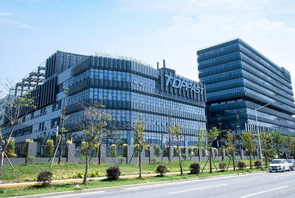
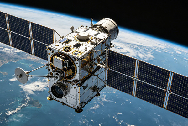
موثوقية عالية مركبات ثنائي الفينيل متعدد الكلور الفضائية الحلول
مصممة خصيصًا للبيئات القاسية. حاصلة على شهادة الامتثال لمعايير AS9100D. نقدم لوحات دوائر مطبوعة خالية تمامًا من العيوب للمهام الحيوية في مجالي الطيران والفضاء على مستوى العالم.
اطلب عرض أسعار فوري
0%
موثوقية المحصول
0+
سنوات الخبرة
0%
إمكانية التتبع الكاملة
لماذا تختار TOPFAST
التصنيع الدقيق للتطبيقات الحيوية.
جودة معتمدة
منشآت حاصلة على شهادتي AS9100D وNADCAP، مما يضمن الامتثال لبروتوكولات الدفاع والطيران الصارمة.
الخبرة المادية
التعامل مع الألواح المركبة عالية الأداء (البولي إيميد، روجرز، PTFE) في البيئات التي تتسم بدرجات حرارة عالية وترددات عالية .
تفتيش صارم
اختبار موثوقية بنسبة 100٪ باستخدام تقنية AOI والأشعة السينية في الوقت الفعلي واختبارات خارج الغلاف الجوي لضمان نتائج خالية من العيوب
طلب عرض أسعار فوري
✓ Direct engineer support
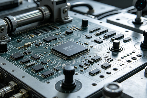
القدرات التقنية
معايير تصنيع دقيقة مُحسَّنة لتناسب ظروف انعدام الجاذبية والبيئات القاسية.
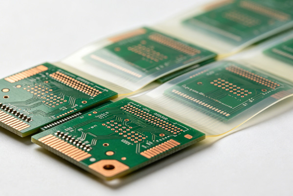
حلول الدوائر الصلبة-المرنة
تقليل كتلة الحمولة مع ضمان موثوقية الاتصال التامة في ظل قوى الجاذبية متعددة الاتجاهات.
ما يصل إلى 24 طبقة
دورة مرونة عالية
تصميم كتاب
محمي من التداخل الكهرومغناطيسي
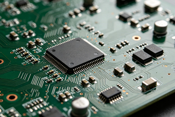
HDI عالي الدقة
توفير وصلات عالية الكثافة لأنظمة التحكم المعقدة ووحدات الرادار و مصفوفات الأقمار الصناعية.
متراكبة ومتداخلة
ELIC لأي طبقة
الملعب فائق الدقة
التحكم في المعاوقة
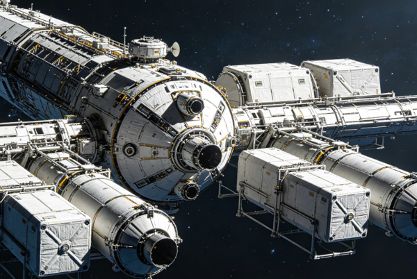
قصص النجاح
تعزيز الموثوقية في أكثر مهام الفضاء صعوبةً على مستوى العالم.
"تُعد شركة TOPFAST المورد الرئيسي لدينا في مجال لوحات الدوائر المطبوعة (PCB) الخاصة بوحدات التحكم في الأقمار الصناعية. إن التزامها بمعايير IPC من الفئة 3/A ثابت لا يتزعزع."
"مستوى التتبع المتاح هو بالضبط ما نحتاجه للمعدات العسكرية. موثق بالكامل ومحترف للغاية."
"مدة إنجاز استثنائية لتصميمات النماذج الأولية المعقدة للأنظمة الصلبة-المرنة. إنها جزء أساسي من خطة عملنا في مجال البحث والتطوير."
"دقة لا تضاهى في الثقوب الدقيقة المتراكبة HDI. وقد وفرت لنا استشاراتهم الفنية أسابيع من عمليات إعادة التصميم المتكررة."
"لقد تعاملت لوحات الركيزة الخزفية الخاصة بهم مع الأحمال الحرارية لوحدات التحكم في الدفع لدينا بشكل مثالي. إنها حقًا ذات جودة مناسبة للفضاء."
المواصفات الفنية والتفاوتات المسموح بها
معايير دقيقة مصممة خصيصًا لتلبية متطلبات قطاعي الفضاء والدفاع.
| معلمات التصنيع | القدرات القياسية | قدرات متطورة |
|---|---|---|
| الحد الأقصى لعدد الطبقات | 2 - 32 طبقة | ما يصل إلى 48 طبقة |
| الحد الأدنى لعرض الخط والمسافة بينه | 3 ميل / 3 ميل | 2 ميل / 2 ميل |
| المواد الأساسية المعتمدة | FR4 (درجة حرارة زجاجية عالية >170)، بوليميد | روجرز، PTFE، أرلون، السيراميك |
| الحد الأدنى لحجم المثقاب | 0.15 مم (حفر ميكانيكي) | 0.075 مم (معالجة بالليزر) |
| تشطيبات الأسطح في مجال الفضاء | ENIG، HASL خالية من الرصاص | ENEPIG، الذهب الصلب، الفضة بالغمر |
| التحكم في مقاومة الإشارة | ± 10% Tolerance | ± 5% Tolerance |
مسار العمل في مجال التصنيع الفضائي
إجراء يخضع لرقابة صارمة ويمكن تتبعه بدقة، بدءًا من مرحلة التصميم الهندسي الأولي وصولاً إلى الفحص المجهري النهائي .
1
تصميم قابل للتصنيع والتحقق من الصحة
تحليل شامل لملفات جيربر والقيود المادية من أجل التنبؤ بنقاط الفشل المحتملة والتخلص منها.
2
مراقبة المواد
الحصول على صفائح قابلة للتتبع بدقة ومطابقة لمعايير صناعة الطيران، تليها عملية تحقق صارمة من المواد الواردة.
3
بريسيشن فاب
معالجة التصوير المباشر بالليزر (LDI)، وتوجيه المقاومة المتخصص، والتصفيح بالفراغ في غرف نظيفة.
4
الاختبارات المتقدمة
اختبار الصدمة الحرارية، وتحليل المقاطع الدقيقة، واختبار شامل للتلوث الأيوني قبل الشحن.
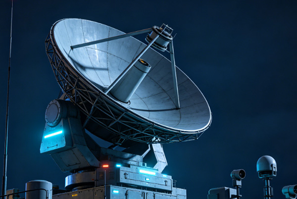
أثبتت كفاءتها في أصعب الظروف
تزويد الجيل القادم من أنظمة إلكترونيات الطيران، وأنظمة التحكم المعقدة في الدفع، والاتصالات الساتلية الآمنة بالطاقة.
الأسئلة المتداولة
نظرة متعمقة على قدراتنا في مجال لوحات الدوائر المطبوعة (PCB) الخاصة بالفضاء الجوي، والالتزام بالمعايير، واستراتيجيات المواد.
ما هي الشهادات في مجال الفضاء الجوي التي تحملها منشآتكم التصنيعية؟
نحن حاصلون على شهادتي AS9100D و ISO9001 بالكامل. علاوة على ذلك، نلتزم التزامًا صارمًا بمعايير IPC من الفئة 3 و
الفئة 3/A
الخاصة بمنتجات الدفاع والفضاء عالية الموثوقية، مما يضمن إدارة جودة استثنائية
وتدقيقًا صارمًا
وشفافية تشغيلية كاملة.
كيف يمكن ضمان التتبع الكامل للمواد المستخدمة في لوحات الدوائر الإلكترونية الخاصة بالفضاء؟
إن إمكانية التتبع أمر غير قابل للتفاوض. نحن نستخدم نظام تخطيط موارد المؤسسات (ERP) مركزيًّا وعالي الأمان يتتبع
كل
دفعة مواد فريدة بدءًا من مصنع المواد الخام المصفحة وصولاً إلى خط التجميع النهائي. ويتم شحن جميع
الألواح
المخصصة للطيران مع شهادة مطابقة (CoC) شاملة وإقرارات كاملة
بالمواد.
هل يمكن للوحات الدوائر المطبوعة الخاصة بكم أن تتحمل درجات الحرارة القصوى والصدمات الحرارية؟
نعم. نحن نعمل بشكل روتيني مع مواد ذات درجة حرارة زجاجية (Tg) عالية جدًا، مثل تركيبات البوليميد المتطورة ومركبات
PTFE
التي صُممت خصيصًا لتحمل التقلبات الحرارية السريعة والشديدة. ويتضمن بروتوكول الاختبار
الداخلي
الخاص بنا إجراء دورات صدمات حرارية قاسية لضمان سلامة الهيكل ضد
التفكك.
هل تقدمون خدمات النماذج الأولية السريعة لمشاريع الفضاء والطيران؟
بالتأكيد. فالابتكار الحقيقي في مجال الفضاء الجوي الحديث يتطلب دورات تطوير مرنة. ونحن ندعم
الإنجاز السريع
لنماذج الاختبار لتسريع مراحل البحث والتطوير لديكم دون المساس أبدًا بالاختبارات الداخلية الصارمة
وفحوصات DRC
والتوثيق المطلوب للانتقال النهائي إلى الأجهزة المخصصة للطيران.
ما هي التشطيبات السطحية التي توصون بها للبيئات المرتفعة؟
فيما يتعلق بالبيئات الفضائية غير المضغوطة، فإننا نطلب عادةً استخدام طلاءات ENIG أو ENEPIG أو الذهب الصلب. وتوفر هذه
الطلاءات المتخصصة عمرًا تخزينيًا طويلاً للغاية، وخصائص ربط أسلاك فائقة، و
مقاومة لا مثيل لها للأكسدة والتآكل في الظروف الجوية القاسية والمتقلبة.