الجيل القادم لوحة الدوائر المطبوعة للاتصالات الحلول
نربط العالم بسرعة الضوء. تصنيع متخصص للوحات الدوائر المطبوعة (PCB) عالية التردد والسرعة، مخصصة للبنية التحتية لشبكات الجيل الخامس (5G) والجيل السادس (6G)، ومراكز البيانات، وشبكات الأقمار الصناعية المتطورة.
اطلب عرض أسعار لخدمات الاتصالات
0جيجابت في الثانية
السرعة في المسار الواحد
0 Df
تبديد طاقة منخفض للغاية
0%
معتمد من PIM و SI
لماذا تختار TOPFAST في مجال الاتصالات
ضمان زمن انتقال منخفض للغاية وعدم حدوث أي تدهور في الإشارة لشبكة الاتصالات العالمية.
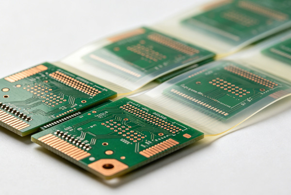
التصفيح الهجين المتخصص
خبرة في ربط طبقات PTFE/Rogers عالية التردد مع مادة FR4 القياسية لتحقيق التوازن بين أداء الطبقات المتعددة والكفاءة من حيث التكلفة.
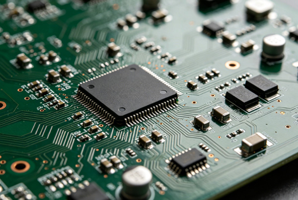
سلامة الإشارة المتقدمة
الاستعانة بتقنية الحفر الخلفي عالية الدقة للتخلص من بقايا الثقوب الموصلة وتقليل انعكاس الإشارات في الدوائر الرقمية عالية السرعة التي تصل سرعتها إلى 112 جيجابت في الثانية.
الاستقرار الحراري للاستخدام في الأماكن المفتوحة
صُممت هذه المنتجات لتتحمل الظروف البيئية القاسية في محطات 5G الخارجية، بفضل نظام إدارة حراري متطور وطلاءات مقاومة للتآكل.
تحدث إلى مهندس اتصالات
✓ Support for Low-PIM Materials
إمكانات على مستوى الشبكات
تميز في التصنيع مُحسَّن ليتناسب مع سعة النقل وترددات معايير الاتصالات الحديثة.
خبراء الترددات الراديوية (RF)
تصنيع مصفوفات هوائيات MIMO الضخمة ووحدات الواجهة الأمامية للترددات اللاسلكية مع تحكم دقيق للغاية في المعاوقة والطور.
±5% Tolerance
ترددات أقل من 6 جيجاهرتز والموجات المليمترية
روجرز، أرلون، PTFE
تصميم منخفض PIM
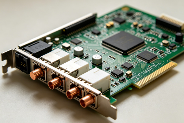
تقنية HSD واللوحة الخلفية
دعم اللوحات الخلفية الرقمية عالية السرعة (HSD) وبطاقات خطوط الشبكات الضوئية التي تتطلب ما يصل إلى 32 طبقة وإمكانية الحفر الخلفي.
ما يصل إلى 48 طبقة
ضبط العمق 0.2 مم
شبكة 800G
التكديس الهجين
ثقة خبراء الشبكات
تصنيع الأجهزة التي تشكل العمود الفقري للاتصالات الرقمية على مستوى العالم.
"Topfast's ability to manufacture hybrid Rogers/FR4 stack-ups with ±5% impedance has been vital for our 5G antenna products."
"لقد فاقت سلامة الإشارة التي حققناها في اللوحة الخلفية المكونة من 32 طبقة، باستخدام عملية الحفر الخلفي التي يقدمونها، توقعاتنا."
"تسليم موثوق به لكميات ضخمة. فقد تمكنوا من التوسع بسلاسة من النماذج الأولية إلى 50 ألف وحدة لمحطات قاعدية."
"تحكم استثنائي في إدارة المعلومات الخاصة بالمنتج (PIM). ويُعد اختيار المواد ونظافة التصنيع لديهم من بين الأفضل في هذا المجال."
"تتميز لوحات الواجهة الضوئية التي تنتجها الشركة بجودة عالية ومستمرة، مما يضمن عدم فقدان أي حزم بيانات في مراكز توزيع البيانات لدينا."
المواصفات الفنية للاتصالات
معلمات متقدمة مُحسَّنة بشكل دقيق للشبكات ذات النطاق الترددي العريض والخسارة المنخفضة.
| معلمات الأداء | قدرات HSD | خيار الترددات اللاسلكية / الموجات المليمترية |
|---|---|---|
| فئة المواد | ميغترون 6/7، تاكيون 100G | RT/duroid، RO4003/4350 |
| القدرة على حساب عدد الطبقات | ما يصل إلى 48 طبقة | ما يصل إلى 12 طبقة (تردد لاسلكي كامل) |
| التحكم في عمق الحفر الخلفي | ± 0.15mm Accu | ± 0.05mm Accu (High Frequency) |
| التحكم في المعاوقة | ± 10% Standard | ± 5% / ± 3% (Precision RF) |
| تشطيب السطح | ENIG، OSP | الفضة المغمورة، الذهب الصلب |
| تقنية "Via-in-Pad" | مملوءة بالراتنج ومغطاة | مملوءة بالراتنج الموصّل |
مسار عمل التصنيع القائم على البيانات لدينا
إجراء يتم التحكم فيه بدقة يركز على سلامة الإشارة وموثوقية الشبكة على المدى الطويل.
1
تحليل SI وتصميم قابل للتصنيع (DFM)
التحقق المتقدم من تراصف المكونات ومحاكاة سلامة الإشارة للتنبؤ بالخسائر وتخفيفها قبل التصنيع.
2
التكديس الهجين
تصفيح دقيق باستخدام دورة حرارية لمواد مختلطة لضمان عدم حدوث أي انفصال في لوحات الترددات اللاسلكية عالية التردد.
3
مصنع خاضع للرقابة
الفحص البصري الآلي (AOI) والنقش بالبلازما لتنظيف الثقوب المارة، يلي ذلك الحفر مع التحكم في العمق.
4
التحقق من SI
اختبار شامل باستخدام تقنية قياس الانعكاس في المجال الزمني (TDR) وتحليل التداخل بين الموجات (PIM) لضمان تحقيق السعة المحددة.
دعم العمود الفقري للاتصال
يتم نشر حلولنا عبر شبكات الطاقة الأكثر أهمية في العالم.


الأسئلة الشائعة حول لوحات الدوائر المطبوعة الخاصة بالاتصالات
أسئلة شائعة حول التصنيع عالي التردد وسلامة الإشارة واستراتيجيات المواد.
كيف يتم التحكم في الحرارة في لوحات الدوائر المطبوعة لمحطات 5G عالية الطاقة؟
نستخدم طبقات نحاسية سميكة (تصل إلى 4 أونصات)، وعملات نحاسية مدمجة، وطبقات مركبة موصلة للحرارة. كما نقوم بتحسين تصميم التراكيب لتوفير تبديد فعال للحرارة إلى الهيكل الخارجي، مما يضمن بقاء المكونات ضمن درجات حرارة التشغيل الآمنة في البيئات الخارجية غير المكيفة.
ما هو نظام إدارة المعلومات المنتج (PIM) ولماذا يعتبر مهمًا في لوحات الدوائر المطبوعة المخصصة للاتصالات؟
يحدث التداخل التوافقي السلبي (PIM) عندما تتسبب عدم الخطية في لوحات الدوائر المطبوعة (PCB) في حدوث تداخل. وفي أنظمة الاتصالات عالية الطاقة، يُعد انخفاض مستوى التداخل التوافقي السلبي (PIM) أمرًا بالغ الأهمية للحفاظ على سعة الشبكة. ونحن نحقق انخفاض مستوى التداخل التوافقي السلبي (PIM) من خلال معالجات متخصصة لرقائق النحاس، واختيار قناع اللحام المناسب، ومستوى نظافة التصنيع وفقًا لمعيار IPC من الفئة 3.
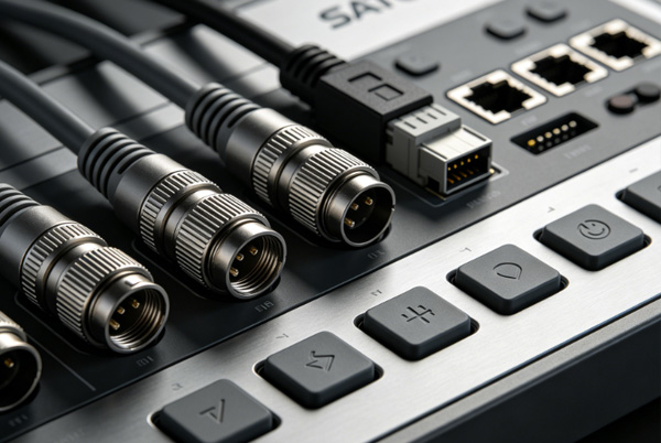
هل تدعم ميزة "back-drilling" في بطاقات خطوط الشبكة؟
Yes. We provide precision back-drilling with depth control of ±0.1mm. This processes removes the unused portions of via stubs, which is essential to prevent reflections and resonance in networking hardware operating at 25Gbps per lane and above.
ما هي المواد التي توصون بها لتصميمات شبكات 800G؟
للحصول على معدل نقل بيانات يبلغ 800 جيجابت (112 جيجابت لكل مسار)، نوصي عادةً باستخدام مواد ذات خسارة منخفضة للغاية مثل Panasonic Megtron 7/8 أو Isola Tachyon 100G أو Park Meteorwave 8000. وتتميز هذه المواد بمعاملات تبديد (Df) منخفضة للغاية وثوابت عازلة (Dk) مستقرة عبر نطاقات تردد واسعة.