Nouvelle génération Circuit imprimé de communication Solutions
Relier le monde à la vitesse de la lumière. Fabrication spécialisée de circuits imprimés haute fréquence et haute vitesse pour les infrastructures 5G/6G, les centres de données et les réseaux satellitaires de pointe.
Demander un devis pour des services de télécommunications
0Gbit/s
Vitesse sur une seule voie
0 Df
Dissipation extrêmement faible
0%
Certifié PIM & SI
Pourquoi choisir TOPFAST pour les télécommunications ?
Garantir une latence extrêmement faible et une dégradation nulle du signal pour le réseau mondial.
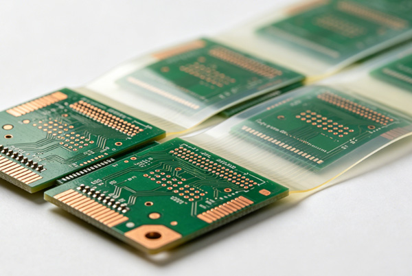
Laminage hybride spécialisé
Expertise dans l'assemblage de couches PTFE/Rogers haute fréquence avec du FR4 standard afin d'optimiser à la fois les performances et la rentabilité des circuits multicouches.
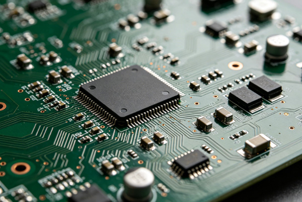
Intégrité avancée du signal
Utilisation d'un perçage arrière de haute précision pour éliminer les résidus de vias et réduire au minimum la réflexion du signal dans les circuits numériques à haute vitesse pouvant atteindre 112 Gbps.
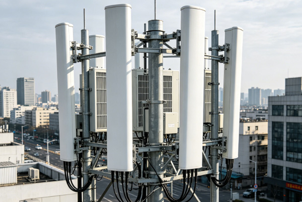
Stabilité thermique pour une utilisation en extérieur
Conçus pour résister aux cycles environnementaux extrêmes dans les stations de base 5G en extérieur, grâce à une gestion thermique de pointe et à des finitions anticorrosion.
Parlez à un ingénieur en télécommunications
✓ Support for Low-PIM Materials
Fonctionnalités de niveau réseau
Une excellence de fabrication optimisée pour le débit et la fréquence des normes de télécommunications modernes.
Experts en radiofréquence (RF)
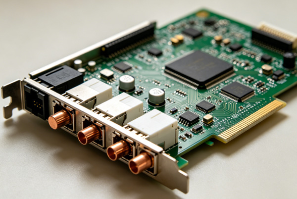
Fabrication de réseaux d'antennes MIMO massifs et de modules de frontal RF avec un contrôle extrêmement précis de l'impédance et de la phase.
±5% Tolerance
Sub-6G et ondes millimétriques
Rogers, Arlon, PTFE
Conception à faible PIM
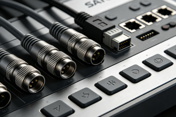
Technologie HSD et de fond de panier
Compatible avec les fonds de panier numériques à haut débit (HSD) et les cartes de réseau optique nécessitant jusqu'à 32 couches et une capacité de perçage arrière.
Jusqu'à 48 couches
Réglage de la profondeur de 0,2 mm
Réseau 800G
Empilage hybride
La confiance des professionnels des réseaux
Nous fabriquons le matériel qui constitue l'épine dorsale des communications numériques à l'échelle mondiale.
"Topfast's ability to manufacture hybrid Rogers/FR4 stack-ups with ±5% impedance has been vital for our 5G antenna products."
« L'intégrité du signal que nous avons obtenue sur notre fond de panier à 32 couches grâce à leur procédé de perçage arrière a dépassé nos attentes. »
« Une livraison fiable pour des volumes considérables. Ils sont passés sans difficulté des prototypes à la production de 50 000 stations de base. »
« Une maîtrise exceptionnelle de la gestion des informations sur les produits (PIM). Le choix des matériaux et la propreté des processus de fabrication sont parmi les meilleurs du secteur. »
« Les cartes d'interface optique qu'ils fabriquent sont d'une qualité constante, garantissant une perte de paquets nulle dans les hubs de notre centre de données. »
Caractéristiques techniques de communication
Paramètres avancés rigoureusement optimisés pour les réseaux à large bande passante et à faibles pertes.
| Paramètre de performance | Capacité HSD | Option RF / ondes millimétriques |
|---|---|---|
| Famille de matériaux | Megtron 6/7, Tachyon 100G | RT/duroid, RO4003/4350 |
| Capacité en termes de nombre de couches | Jusqu'à 48 couches | Jusqu'à 12 couches (RF complet) |
| Contrôle de la profondeur de perçage en contre-sens | ± 0.15mm Accu | ± 0.05mm Accu (High Frequency) |
| Contrôle de l'impédance | ± 10% Standard | ± 5% / ± 3% (Precision RF) |
| Finition de la surface | ENIG, OSP | Argent par immersion, or dur |
| Technologie Via-in-Pad | Rempli de résine et coiffé | Rempli de résine conductrice |
Notre processus de fabrication basé sur les données
Une procédure rigoureusement contrôlée, axée sur l'intégrité du signal et la fiabilité à long terme du réseau.
1
Analyse SI et conception pour la fabrication (DFM)
Vérification avancée de l'empilement et simulation de l'intégrité du signal pour anticiper et limiter les pertes avant la fabrication.
2
Empilage hybride
Laminage par cycles thermiques précis de matériaux mixtes afin de garantir l'absence totale de délamination dans les cartes RF haute fréquence.
3
Usine sous contrôle
Inspection optique automatique (AOI) et gravure au plasma pour obtenir des trous de passage propres, suivis d'un perçage avec contrôle de la profondeur.
4
Vérification SI
Tests complets par réflectométrie dans le domaine temporel (TDR) et analyse des interférences de port (PIM) afin de garantir le débit spécifié.
Au cœur de la connectivité
Nos solutions sont déployées sur les réseaux électriques les plus critiques au monde.


FAQ sur les circuits imprimés pour les télécommunications
Questions fréquentes sur la fabrication haute fréquence, l'intégrité du signal et les stratégies en matière de matériaux.
Comment gérez-vous la dissipation thermique dans les circuits imprimés des stations de base 5G à haute puissance ?
Nous utilisons des couches de cuivre épaisses (jusqu'à 4 oz), des pastilles de cuivre intégrées et des stratifiés thermoconducteurs. Nous optimisons également les empilages afin d'assurer une dissipation efficace de la chaleur vers le châssis externe, garantissant ainsi que les composants restent dans des plages de températures de fonctionnement sûres dans des environnements extérieurs non climatisés.
Qu'est-ce que le PIM et pourquoi est-il important pour les circuits imprimés de communication ?
L'intermodulation passive (PIM) se produit lorsque les non-linéarités présentes dans le circuit imprimé génèrent des interférences. Dans les systèmes de télécommunications à haute puissance, un faible niveau de PIM est essentiel pour préserver la capacité du réseau. Nous parvenons à réduire le PIM grâce à des traitements spécifiques de la feuille de cuivre, au choix du masque de soudure et à une propreté de fabrication conforme à la norme IPC Classe 3.
Prend-il en charge le perçage arrière pour les cartes réseau ?
Yes. We provide precision back-drilling with depth control of ±0.1mm. This processes removes the unused portions of via stubs, which is essential to prevent reflections and resonance in networking hardware operating at 25Gbps per lane and above.
Quels composants recommandez-vous pour les configurations réseau 800G ?
Pour un débit de 800 G (112 G par voie), nous recommandons généralement des matériaux à très faible perte, tels que le Panasonic Megtron 7/8, l'Isola Tachyon 100G ou le Park Meteorwave 8000. Ceux-ci offrent des facteurs de dissipation (Df) exceptionnellement bas et des constantes diélectriques (Dk) stables sur de larges plages de fréquences.