Haute densité Cartes de circuits imprimés pour l'électronique grand public Solutions
Au cœur de la prochaine génération d'appareils intelligents. Solutions HDI de précision et rigide-flex pour les smartphones, les appareils portables et les écosystèmes de l'Internet des objets.
Demandez un devis instantané
0%
L'excellence en matière de rendement
0+
Années d'expérience
0h
Prototypage rapide
Pourquoi choisir TOPFAST pour l'électronique grand public ?
Favoriser l'innovation grâce à la miniaturisation, aux performances à haut débit et à une production de masse rentable.

Expertise en miniaturisation
Une technologie HDI de pointe, avec des microvias sur toutes les couches, permettant d'intégrer des circuits complexes dans des boîtiers élégants et compacts.
Optimisation du rapport coût-performance
Des processus de fabrication rationalisés, conçus pour offrir des produits de qualité supérieure à des prix compétitifs.
Chaîne logistique agile
Des capacités de production évolutives, allant du prototypage rapide à la production en grande série, afin de répondre aux demandes saisonnières.
Demande de devis immédiat
✓ ISO 9001 & UL Certified Production
Compétences techniques des consommateurs
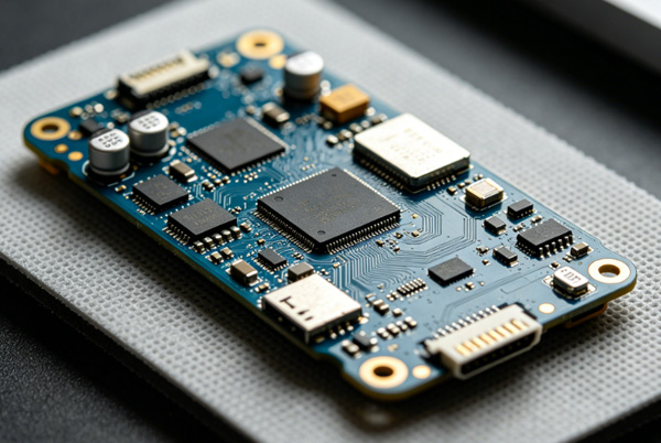
Prise en charge d'appareils portables haute performance et d'appareils domestiques intelligents grâce à des interconnexions à haute densité.
Appareils mobiles et portables
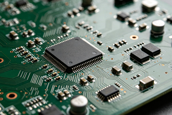
Spécialisé dans les circuits imprimés HDI à n'importe quel nombre de couches et les substrats minces destinés aux smartphones, tablettes et consoles de jeux.
Tout niveau / ELIC
2 km / 2 km
D'une épaisseur de 0,2 mm
ENIG / OSP
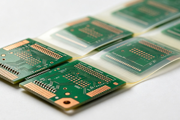
Appareils portables intelligents et Internet des objets
Circuits imprimés flexibles et flex-rigides conçus pour les formes courbes et une intégration durable dans des appareils portables fonctionnant 24 heures sur 24, 7 jours sur 7.
Circuit imprimé rigide-flex multicouche
Assemblage en surface haute densité
Perçage au laser
Base en polyimide (PI)
Partenaires dans le domaine des technologies grand public
« Leur capacité à gérer des circuits imprimés HDI à n'importe quel nombre de couches pour notre smartphone phare était impressionnante. L'intégrité du signal est excellente, même à des vitesses élevées. »
« La conception « rigid-flex » qu'ils nous ont proposée pour notre dernière montre connectée nous a permis de réduire l'épaisseur de l'appareil de 15 %. Je les recommande vivement. »
« Le prototypage rapide nous a permis de respecter le calendrier de lancement de notre produit. Leurs conseils en matière de conception pour la fabrication nous ont fait gagner deux semaines de révisions de conception. »
« La constance dans la production de masse est essentielle pour nous. Grâce à Topfast, nous sommes passés de 1 000 à 100 000 unités sans aucune baisse de qualité. »
« Une finition soignée et un contrôle qualité à 100 %. Depuis que nous avons adopté Topfast, le taux de produits défectueux à la livraison de nos tablettes grand public a considérablement diminué. »
« Une communication professionnelle et un excellent soutien technique pour la transition vers des matériaux sans halogène. Idéal pour nos initiatives écologiques. »
Spécifications et normes relatives aux circuits imprimés grand public
| Paramètres | Consommateur lambda | Appareil haut de gamme (HDI) |
|---|---|---|
| Matériau de base | FR4 (standard) | Sans halogène, résine BT, PI |
| Épaisseur du cuivre | Une demi-once - une once | Jusqu'à 85 g (en charge rapide) |
| Traitement de surface | OSP / ENIG | ENEPIG / Étain par immersion |
| Min Trace/Espace | 3 / 3 km | 1,5 / 1,5 mil (pas fin) |
| Validation | CE / FCC / RoHS | Blindage contre les interférences électromagnétiques / Interconnexions à haut débit |
| Contrôle de la qualité | Classe 2 de l'IPC | Prise en charge des classes IPC 2 et 3 |
Processus de fabrication agile
1
Commentaires sur la conception
Analyse DFM immédiate visant à optimiser une production en série compacte et à haut rendement.
2
HDI de précision
Impression directe par laser et perçage de microvias pour des circuits mobiles de pointe.
3
Intégrité du signal
Tests avancés de contrôle d'impédance pour garantir une connectivité 5G et Wi-Fi irréprochable.
4
Inspection finale
Contrôles AOI et tests électriques à 100 % pour garantir la fiabilité des produits une fois entre les mains des consommateurs.
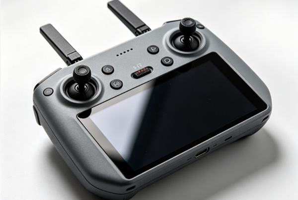
Applications dans la vie quotidienne

FAQ sur les circuits imprimés grand public
Quel est votre délai d'exécution le plus court pour les prototypes destinés aux consommateurs ?
Nous proposons un service de prototypage rapide en 24 heures pour les cartes standard à deux couches et en 2 à 4 jours pour les conceptions HDI multicouches complexes, afin de vous aider à accélérer votre développement.
Prend-vous en charge les circuits imprimés HDI à n'importe quel nombre de couches pour les appareils ultra-minces ?
Oui. Nous sommes spécialisés dans la technologie ELIC (Every Layer Interconnect), qui permet d'atteindre une densité de circuits maximale dans les smartphones fins et les appareils électroniques portables.
Êtes-vous en mesure de gérer une production à grand volume pour le lancement de nouveaux produits ?
Tout à fait. Nos installations sont conçues pour s'adapter à toutes les échelles, qu'il s'agisse du lancement de nouveaux produits (NPI) ou de la production en série à grand volume, tout en garantissant une qualité constante.
Vos matériaux sont-ils conformes aux directives RoHS et REACH ?
Oui, tous nos matériaux et finitions de surface standard destinés à l'électronique grand public sont pleinement conformes aux réglementations environnementales RoHS et REACH.