Alta densidad Electrónica de consumo PCB Soluciones
Impulsando la próxima generación de dispositivos inteligentes. Soluciones HDI de precisión y Rigid-Flex para smartphones, dispositivos wearables y ecosistemas del IoT.
Solicita un presupuesto al instante
0%
Excelencia en el rendimiento
0+
Años de experiencia
0h
Creación rápida de prototipos
¿Por qué elegir TOPFAST para la electrónica de consumo?
Impulsamos la innovación mediante la miniaturización, el rendimiento de alta velocidad y la producción en masa rentable.

Experiencia en miniaturización
Tecnología HDI líder en el sector con microvías en cualquier capa, que permite integrar circuitos complejos en carcasas elegantes y compactas.
Optimización de la relación calidad-precio
Procesos de fabricación optimizados, diseñados para ofrecer productos de primera calidad a precios competitivos.
Cadena de suministro ágil
Capacidades de producción escalables que van desde la creación rápida de prototipos hasta la producción a gran escala para satisfacer las demandas estacionales.
Solicitar presupuesto instantáneo
✓ ISO 9001 & UL Certified Production
Capacidades técnicas de los consumidores
Compatibilidad con dispositivos portátiles de alto rendimiento y dispositivos domésticos inteligentes mediante interconexiones de alta densidad.
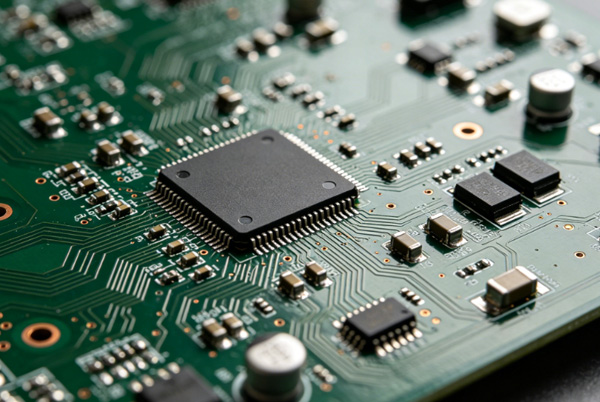
Dispositivos móviles y portátiles
Especializados en HDI de cualquier número de capas y sustratos finos para teléfonos inteligentes, tabletas y consolas de videojuegos.
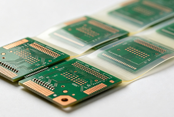
Cualquier capa / ELIC
2 millas / 2 millas
De tan solo 0,2 mm de grosor
ENIG / OSP
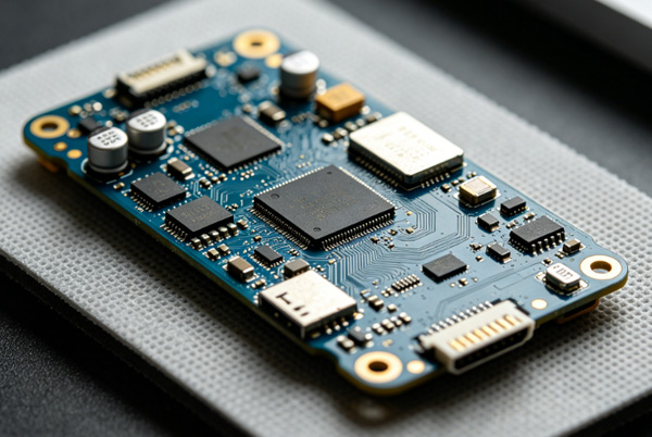
Dispositivos inteligentes y el Internet de las cosas
Circuitos impresos flexibles y rígido-flexibles diseñados para formas curvas y una integración duradera en dispositivos wearables que funcionan las 24 horas del día, los 7 días de la semana.
Rígido-flexible multicapa
SMT de alta densidad
Perforado con láser
Base de poliimida (PI)
Socios en tecnología de consumo
«Su capacidad para gestionar circuitos impresos de alta densidad (HDI) de cualquier número de capas para nuestro smartphone insignia fue impresionante. La integridad de la señal es excelente incluso a altas velocidades».
«El diseño rígido-flexible que nos proporcionaron para nuestro último reloj inteligente nos permitió reducir el grosor del dispositivo en un 15 %. Muy recomendable».
«La creación rápida de prototipos nos ayudó a cumplir con el plazo de lanzamiento del producto. Sus comentarios sobre la fabricación nos ahorraron dos semanas de revisiones de diseño».
«La uniformidad en la producción en serie es fundamental para nosotros. Hemos pasado de fabricar 1 000 a 100 000 unidades con Topfast sin que la calidad se haya visto afectada en absoluto».
«Acabados de calidad y pruebas al 100 %. Desde que cambiamos a Topfast, nuestras tabletas para el gran público han registrado una reducción significativa en las tasas de productos defectuosos al recibir el pedido».
«Una comunicación profesional y un excelente soporte técnico para la transición a materiales sin halógenos. Perfecto para nuestras iniciativas ecológicas.»
Especificaciones y normas para placas de circuito impreso de consumo
| Parámetro | Consumidor estándar | Dispositivo de gama alta (HDI) |
|---|---|---|
| Material de base | FR4 (estándar) | Sin halógenos, resina BT, PI |
| Espesor del cobre | Media onza - una onza | Hasta 85 g (carga rápida) |
| Tratamiento de superficies | OSP / ENIG | ENEPIG / Estaño por inmersión |
| Traza mínima/Espacio | 3 / 3 millas | 1,5 / 1,5 mil (paso fino) |
| Validación | CE / FCC / RoHS | Protección contra interferencias electromagnéticas / Interconexiones de alta velocidad |
| Control de calidad | Clase 2 del IPC | Compatibilidad con las clases 2 y 3 del IPC |
Flujo de trabajo de fabricación ágil
1
Comentarios sobre el diseño
Análisis inmediato de DFM para optimizar una producción en serie compacta y de alto rendimiento.
2
HDI de precisión
Impresión directa por láser y perforación de microvías para circuitos móviles de última generación.
3
Integridad de la señal
Pruebas avanzadas de control de impedancia para garantizar una conectividad 5G y Wi-Fi impecable.
4
Inspección final
Pruebas AOI y eléctricas al 100 % para garantizar la fiabilidad del producto en manos del consumidor.
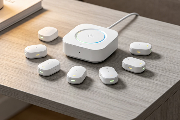
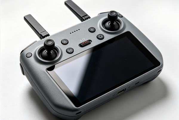
Aplicaciones en la vida cotidiana
Preguntas frecuentes sobre placas de circuito impreso para consumidores
¿Cuál es vuestro plazo de entrega más rápido para prototipos destinados al consumidor?
Ofrecemos un servicio de prototipado rápido en 24 horas para placas estándar de dos capas y de 2 a 4 días para diseños HDI multicapa complejos, con el fin de ayudarte a acelerar el desarrollo.
¿Admiten placas HDI de cualquier número de capas para dispositivos ultradelgados?
Sí. Nos especializamos en la tecnología ELIC (Every Layer Interconnect), que permite alcanzar la máxima densidad de circuitos en smartphones de perfil fino y dispositivos electrónicos portátiles.
¿Podéis hacer frente a una producción a gran escala para el lanzamiento de productos?
Por supuesto. Nuestras instalaciones están preparadas para adaptarse a cualquier volumen de producción, desde la introducción de nuevos productos (NPI) hasta la fabricación en serie a gran escala, siempre con una calidad constante.
¿Cumplen sus materiales con las normativas RoHS y REACH?
Sí, todos nuestros materiales y acabados estándar para productos electrónicos de consumo cumplen plenamente con las normativas medioambientales RoHS y REACH.