Alta densidade PCB de eletrônicos de consumo Soluções
Impulsionando a próxima geração de dispositivos inteligentes. Soluções HDI de precisão e Rigid-Flex para smartphones, dispositivos vestíveis e ecossistemas de IoT.
Solicite um orçamento instantâneo
0%
Excelência em Rendimento
0+
Anos de experiência
0h
Prototipagem rápida
Por que escolher a TOPFAST para produtos eletrônicos de consumo
Impulsionando a inovação por meio da miniaturização, do desempenho em alta velocidade e da produção em massa com boa relação custo-benefício.

Experiência em miniaturização
Tecnologia HDI líder do setor, com microvias em qualquer camada, para acomodar circuitos complexos em caixas elegantes e compactas.
Otimização da relação custo-desempenho
Processos de fabricação otimizados, concebidos para oferecer produtos de alta qualidade a preços competitivos no mercado.
Cadeia de Suprimentos Ágil
Capacidades de produção escaláveis que vão desde a prototipagem rápida até a produção em grande volume, para atender às demandas sazonais.
Solicite uma cotação instantânea
✓ ISO 9001 & UL Certified Production
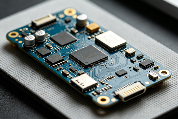
Competências técnicas do consumidor
Oferecendo suporte a dispositivos portáteis de alto desempenho e dispositivos domésticos inteligentes por meio de interconexões de alta densidade.
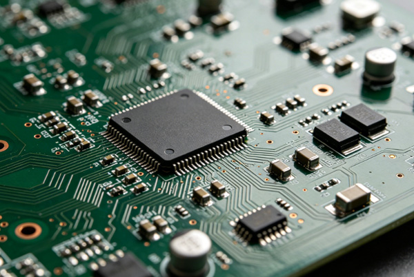
Dispositivos móveis e portáteis
Especializada em HDI de qualquer número de camadas e substratos finos para smartphones, tablets e consoles de videogame.
Qualquer camada / ELIC
2 milhas / 2 milhas
Com espessura de apenas 0,2 mm
ENIG / OSP
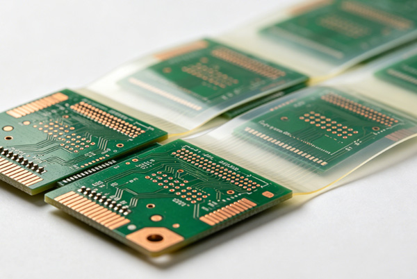
Dispositivos vestíveis inteligentes e IoT
PCBs flexíveis e rígido-flexíveis projetadas para formatos curvos e integração durável em dispositivos vestíveis 24 horas por dia, 7 dias por semana.
Rígido-flexível multicamadas
SMT de alta densidade
Perfurado a laser
Base de poliimida (PI)
Parceiros de Tecnologia de Consumo
"A capacidade deles de lidar com placas HDI de qualquer número de camadas para o nosso smartphone carro-chefe foi impressionante. A integridade do sinal é excelente, mesmo em altas velocidades."
"O projeto Rigid-Flex que eles forneceram para o nosso mais recente smartwatch nos permitiu reduzir a espessura do dispositivo em 15%. Altamente recomendado."
"A prototipagem rápida nos ajudou a cumprir o prazo de lançamento do produto. O feedback sobre DFM (Design for Manufacturing) nos poupou duas semanas de revisões no projeto."
"A consistência na produção em massa é fundamental para nós. Passamos de 1 mil para 100 mil unidades com a Topfast, sem nenhuma perda de qualidade."
"Acabamento de qualidade e testes a 100%. Nossos tablets para o consumidor tiveram uma redução significativa nas taxas de produtos com defeito de fábrica desde que passamos a utilizar a Topfast."
"Comunicação profissional e excelente suporte técnico para a transição para materiais sem halogênio. Perfeito para nossas iniciativas ecológicas."
Especificações e normas para placas de circuito impresso (PCB) de consumo
| Parâmetro | Consumidor comum | Dispositivo de alta qualidade (HDI) |
|---|---|---|
| Material de base | FR4 (padrão) | Sem halogênio, resina BT, PI |
| Espessura do cobre | Meia onça - uma onça | Até 85 g (carregamento rápido) |
| Tratamento de superfície | OSP / ENIG | ENEPIG / Estanho por imersão |
| Traço/Espaço mínimo | 3 / 3 mil | 1,5 / 1,5 mil (passo fino) |
| Validação | CE / FCC / RoHS | Proteção contra interferências eletromagnéticas / Interconexão de alta velocidade |
| Controle de qualidade | Classe 2 da IPC | Suporte para as classes 2 e 3 da IPC |
Fluxo de trabalho de fabricação ágil
1
Comentários sobre o design
Análise imediata de DFM para otimizar a produção em massa compacta e de alto rendimento.
2
HDI de precisão
Imagem direta a laser e perfuração de microvias para circuitos móveis de última geração.
3
Integridade do sinal
Testes avançados de controle de impedância para garantir uma conectividade 5G e Wi-Fi impecável.
4
Inspeção final
Testes 100% AOI e elétricos para garantir a confiabilidade do produto nas mãos dos consumidores.
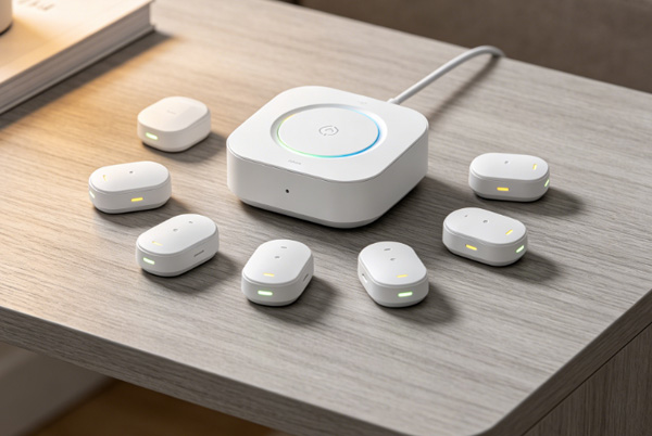
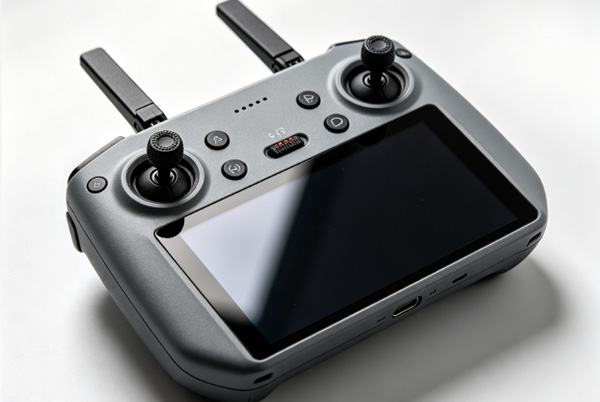
Aplicações na vida cotidiana
Perguntas frequentes sobre placas de circuito impresso para consumidores
Qual é o prazo de entrega mais rápido para protótipos de produtos de consumo?
Oferecemos um serviço de prototipagem rápida em 24 horas para placas padrão de duas camadas e em 2 a 4 dias para projetos HDI complexos de várias camadas, a fim de ajudar você a acelerar o desenvolvimento.
Vocês oferecem suporte a HDI de qualquer camada para dispositivos ultrafinos?
Sim. Somos especializados na tecnologia ELIC (Every Layer Interconnect), que permite a máxima densidade de circuitos em smartphones finos e dispositivos eletrônicos vestíveis.
Vocês têm capacidade para lidar com a produção em grande escala para o lançamento de produtos?
Com certeza. Nossas instalações estão preparadas para operar em grande escala, oferecendo suporte a todas as etapas, desde a introdução de novos produtos (NPI) até a produção em massa de alto volume, com qualidade consistente.
Os seus materiais estão em conformidade com as normas RoHS e REACH?
Sim, todos os nossos materiais padrão e acabamentos de superfície para produtos eletrônicos de consumo estão em total conformidade com as regulamentações ambientais RoHS e REACH.