De alta precisión Placa de circuito impreso para hogar inteligente Soluciones
Impulsamos la próxima generación del IoT. Desde dispositivos wearables compactos hasta complejos centros de control inteligentes, ofrecemos circuitos fiables y de alta densidad para un mundo perfectamente conectado.
Obtén un presupuesto al instante
0%
Rendimiento de fabricación
0 Días
Plazo de entrega del prototipo
0M+
Capacidad mensual
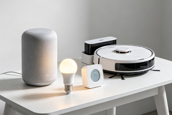
La Fundación Smart Home
Llevar tus innovaciones en el ámbito del IoT desde la fase de prototipo rápido hasta el mercado masivo.

Optimización inalámbrica
Experiencia especializada en control de impedancia y apilamiento para módulos inalámbricos Matter, Thread, WiFi 6 y Zigbee.
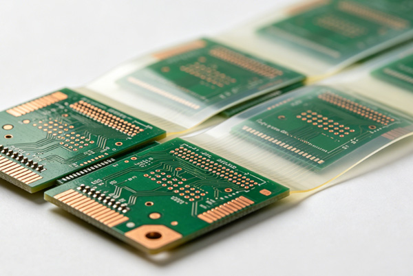
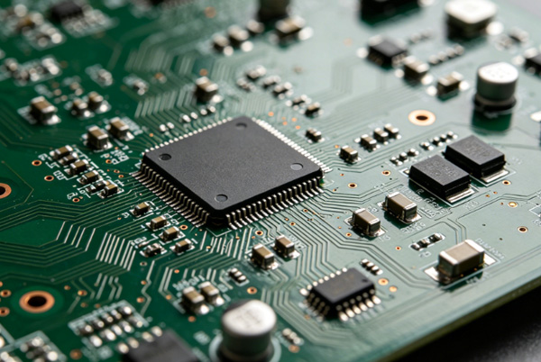
HDI ultracompacto
Compatible con microvías de 0,1 mm y la tecnología Any-Layer para integrar controles inteligentes complejos en carcasas de dispositivos minimalistas.
Materiales ecológicos
Fabricación conforme a las normativas RoHS y REACH con laminados sin halógenos aptos para entornos de electrónica de consumo.
Solicitar presupuestos para placas de circuito impreso
✓ Global shipping within 48 hours
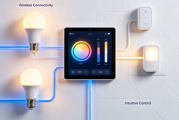
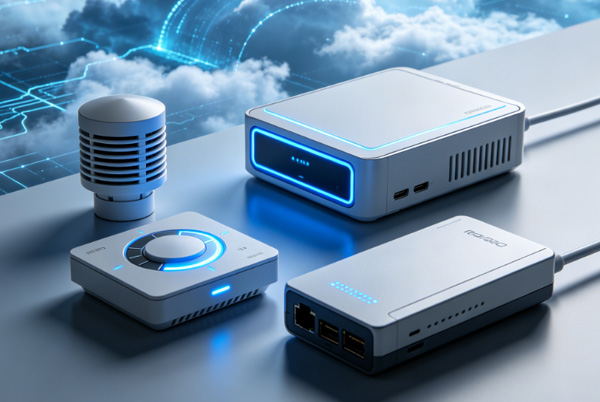
Funcionalidades preparadas para el IoT
Normas de fabricación optimizadas para dispositivos domésticos inteligentes compactos y de bajo consumo.
Tecnología inalámbrica y de radiofrecuencia
Garantizar la integridad absoluta de la señal en redes en malla de bajo consumo y transmisiones multimedia de gran ancho de banda.
2,4 GHz / 5,8 GHz
Maquetas
Baja pérdida (Rogers)
Sin pérdida de señal
Conectividad flexible
Combinación de sustratos rígidos y flexibles para cámaras plegables, sensores inteligentes y dispositivos wearables ergonómicos.
Espesor mínimo: 0,1 mm
ELIC para cualquier capa
SMT de paso fino
FPC con clasificación IP67
Historias de éxito de innovadores
Hacemos realidad los conceptos de vida inteligente con hardware de calidad profesional.
«Su experiencia en HDI nos permitió reducir el tamaño de nuestro termostato inteligente en un 40 % sin perder funcionalidad. El alcance de la señal es impecable».
«Topfast es nuestra opción preferida para la creación rápida de prototipos de IoT. Pasamos del diseño a un prototipo funcional en solo cinco días».
«La calidad de sus placas rígido-flexibles para nuestras cámaras con cerradura inteligente es excepcional. Son duraderas y muy fiables».
«Un apoyo excepcional durante la fase de DFM. Detectaron un problema de espaciado entre las pistas que nos ahorró miles de euros en residuos».
«Su capacidad para gestionar la producción en masa a gran escala ha sido fundamental para el lanzamiento mundial de nuestro producto este año».
Parámetros técnicos de las placas de circuito impreso para el IoT
Especificaciones estándar y avanzadas diseñadas específicamente para la tecnología inteligente de consumo y doméstica.
| Parámetro de especificación | Funcionalidad estándar | Opción avanzada |
|---|---|---|
| Número máximo de capas | 2 - 16 capas | Hasta 32 capas |
| Ancho mínimo de línea / Espaciado | 3,5 millas / 3,5 millas | 2,5 millas / 2,5 millas |
| Opciones de material base | FR4 (estándar y TG150) | Poliimida, alta frecuencia |
| Acabados superficiales | HASL sin plomo, OSP | ENIG (oro), plata por inmersión |
| A través de la tecnología | 0,2 mm (mecánico) | 0,1 mm (microvía láser) |
| Grosor del tablero | 0,4 mm - 1,6 mm | A medida (0,1 mm - 3,2 mm) |
Nuestro flujo de trabajo de fabricación para el IoT
Un proceso optimizado y automatizado diseñado para una rápida escalabilidad y una calidad constante.
1
Validación del diseño
Revisión inmediata del diseño para la fabricación (DFM) con el fin de garantizar la integridad de la antena inalámbrica y la eficiencia en la fabricación.
2
Creación rápida de prototipos
Fabricación en plazos de entrega de 24 a 48 horas para sus fases de I+D y pruebas de campo.
3
Fábrica automatizada
Fabricación en serie mediante líneas automatizadas de alta velocidad con inspección óptica AOI al 100 %.
4
Garantía de calidad
Pruebas de conformidad con la norma IPC-6012 Clase 2, pruebas eléctricas y verificación de la resistencia a la humedad.
Energía para el hogar moderno
Nuestros circuitos impresos son el corazón de millones de dispositivos inteligentes en todo el mundo.

Preguntas frecuentes sobre placas de circuito impreso para hogares inteligentes
Preguntas frecuentes sobre la fabricación de placas de IoT y las capacidades de producción en serie.
¿Ofrecen servicios de fabricación de placas de circuito impreso con antenas inalámbricas integradas?
Yes, we have extensive experience in fabricating PCBs with PCB-trace antennas, chip antennas, and integrated RF modules. We ensure precise impedance control (typically ±10% or ±5%) for optimal signal range and reliability.
¿Cuál es la cantidad mínima de pedido para proyectos de domótica?
Ofrecemos servicios que abarcan desde un único prototipo (pedido mínimo de 1 unidad) hasta la producción en serie de millones de unidades. Nuestras instalaciones están diseñadas para adaptarse perfectamente a las distintas fases de su proyecto.
¿Podrías ayudarnos con la miniaturización de nuestros aparatos electrónicos domésticos?
Por supuesto. Gracias al uso de la tecnología HDI (High-Density Interconnect), las microvías apiladas y el montaje SMT de paso fino, podemos reducir considerablemente el tamaño de su placa de circuito impreso sin comprometer la potencia de procesamiento ni la conectividad.
¿Cumplen tus placas de circuito impreso con las normas internacionales de seguridad para el consumidor?
Sí. Nuestra fábrica cuenta con la certificación UL (E353422) y todos nuestros productos cumplen con las normativas RoHS y REACH. Además, seguimos las normas IPC-A-600/610 de Clase 2 como referencia para la electrónica de consumo, y ofrecemos la Clase 3 para dispositivos médicos de alta fiabilidad.