Haute précision Circuit imprimé pour semi-conducteurs Solutions
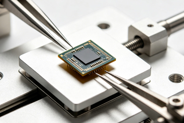
Repousser les limites de la microélectronique. Nous proposons des solutions de circuits imprimés à très grand nombre de couches et à pas fin pour les tests de circuits intégrés, les cartes de sondes et les applications au niveau du substrat.
Demander un devis technique
0+
Capacité en termes de nombre de couches
0mm
Support de pas minimal
0%
Testé par micro-section
Pourquoi choisir TOPFAST pour les semi-conducteurs ?
L'excellence technique au service des architectures silicium les plus complexes au monde.

Densité de couches extrêmement élevée
Spécialisé dans la fabrication de cartes épaisses à grand nombre de couches (jusqu'à 8,0 mm d'épaisseur) destinées aux cartes de charge complexes et aux cartes de sondes.
Experts en gestion thermique
Maîtrise des technologies de pointe en matière de pièces en cuivre et de stratifiés à haute conductivité thermique destinés aux environnements d'essais de rodage à haute puissance.
Alignement de précision nanométrique
En utilisant des systèmes LDI haut de gamme et des techniques d'alignement spécialisées pour garantir un repérage parfait entre des dizaines de couches de signaux.
Devis d'ingénierie instantané
✓ Support for ENEPIG & Hard Gold
Capacités pour l'industrie des semi-conducteurs
Normes de fabrication de précision optimisées pour les essais à tolérance zéro et les applications sur substrat.
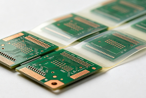
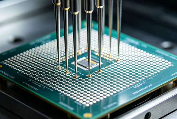
Cartes d'interface de test pour circuits intégrés
Fabrication spécialisée de cartes de charge et de cartes DUT (Device Under Test) présentant des finitions de surface extrêmement planes et des pastilles BGA à pas fin.
Jusqu'à 20:1
Min. 0,3 mm
Jusqu'à 8,0 mm
Planar ENEPIG
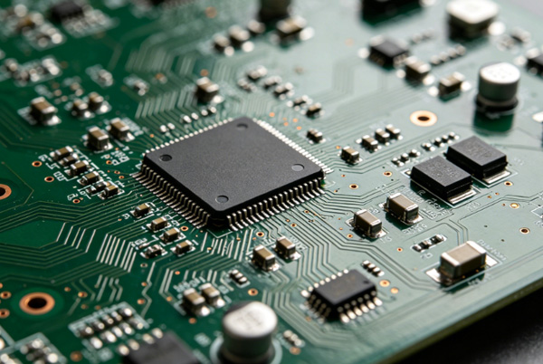
Cartes de test avancées
Nous fournissons le matériel essentiel pour les tests au niveau de la plaquette, doté d'interconnexions verticales à haute densité et d'une stabilité mécanique supérieure.
Faible temps de propagation
Reconstruction hybride
Contrôle du perçage en retrait
PTFE à très faible perte
Fiducie sectorielle
Accompagner l'ensemble de la chaîne d'approvisionnement, des sociétés de conception sans usine aux centres de test internationaux.
« Topfast est l'un des rares fournisseurs capables de fournir des cartes de chargement de plus de 40 couches avec la précision d'alignement requise par nos tests de GPU. »
« La qualité de leur finition ENEPIG et la planéité de leurs pastilles sont idéales pour le montage de nos connecteurs BGA à grand nombre de broches. »
« Leurs conseils techniques lors de la conception de notre carte de rodage à haute puissance nous ont évité une défaillance thermique majeure. »
« Des délais d'exécution imbattables pour les prototypes multicouches. Ils comprennent l'urgence des cycles de lancement dans le secteur des semi-conducteurs. »
« Leur capacité à réaliser des perçages arrière à fort rapport d'aspect est essentielle pour répondre à nos exigences en matière d'intégrité du signal à haute vitesse. »
Spécifications des circuits imprimés pour semi-conducteurs
Paramètres de fabrication extrêmes, strictement adaptés aux tests et à la fiabilité des circuits intégrés.
| Paramètres | Performances de haut niveau | Option ultra-précision |
|---|---|---|
| Nombre maximal de couches | 32 à 40 couches | Jusqu'à 64 calques |
| Largeur minimale des lignes / Espacement | 2,5 km / 2,5 km | 1,8 km / 1,8 km (SLP) |
| Rapport d'aspect du forage | 12:1 | 20:1 (panneaux ultra-épais) |
| Planéité de la surface | < 5µm Tolerance | < 2µm (Laser Leveling) |
| Familles de matériaux | FR4 à haute température de transition vitreuse, Megtron 6/7 | Tachyon 100G, Isola Terra |
| Finition de la surface | ENIG / Or dur | ENEPIG / Or sélectif |
Notre processus de fabrication de composants électroniques de qualité IC
Un processus en plusieurs étapes et à haute résolution garantissant un matériel d'interface sans défaut.
1
Validation SI/PI
Simulation rigoureuse de l'intégrité du signal et de l'alimentation afin de garantir que la conception est capable de gérer les charges des circuits intégrés à haute fréquence.
2
Laser Fab
Perçage et imagerie laser submicroniques pour la création d'interconnexions ultrafines destinées aux substrats de cartes de sondes.
3
Contrôle vertical
Procédés de cuivrage spécialisés visant à garantir une impédance homogène sur les vias à fort rapport d'aspect.
4
Analyse finale
Contrôle optique automatique (AOI) en 3D et analyse à 100 % des micro-coupes pour vérifier l'alignement interne et la stabilité thermique.
À la pointe de l'innovation dans le domaine des semi-conducteurs
Nos circuits imprimés sont au cœur des processus de test et de validation du matériel informatique de nouvelle génération.

FAQ sur les circuits imprimés pour semi-conducteurs
Aperçu de la fabrication de circuits imprimés à grand nombre de couches et des équipements de contrôle de précision.
Comment garantissez-vous la précision de l'enregistrement sur des cartes de plus de 40 couches ?
Nous utilisons des systèmes Mass Lam à la pointe de la technologie, équipés de forage aux rayons X et d'imagerie LDI. Nos conditions environnementales sont rigoureusement maintenues selon les normes des salles blanches de classe ISO 5 pour ces couches, afin d'éviter tout déséquilibre de dilatation thermique ou toute contamination par la poussière pendant le cycle de laminage.
Pouvez-vous traiter du cuivre ultra-épais pour des cartes de rodage à haute puissance ?
Oui, nous prenons en charge des couches de cuivre épais pouvant atteindre 10 oz pour les couches de distribution d'énergie. Nous intégrons également des pastilles de cuivre et des dissipateurs thermiques directement dans la structure du circuit imprimé afin de gérer les charges thermiques extrêmes lors des tests de puces soumis à des contraintes élevées.
Quelle est votre capacité en matière d'intégrité du signal à haute vitesse ?
Nous proposons un perçage arrière de pointe permettant d'éliminer les résidus de vias, et nous travaillons avec une large gamme de matériaux à faible constante diélectrique (DK) et faible facteur de dissipation (DF), tels que le Panasonic Megtron 7 et l'Isola Tachyon. Nous garantissons une propagation du signal homogène sur l'ensemble de l'interface de la carte de test, pour des débits pouvant atteindre 112 Gbps.
Proposez-vous des analyses par microcoupe pour les produits destinés à l'industrie des semi-conducteurs ?
Standard. Chaque commande de circuits imprimés pour semi-conducteurs comprend un rapport détaillé sur les micro-coupes, les résultats des essais de coupons de contrainte thermique et une analyse complète de la contamination ionique, le tout faisant partie de notre documentation d'expédition (CoC).