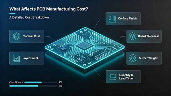
Lorsque les ingénieurs demandent un devis pour un circuit imprimé, le prix final peut parfois s'avérer très différent de ce à quoi ils s'attendaient au départ.
Deux cartes aux dimensions similaires peuvent présenter des coûts de fabrication totalement différents, car leurs structures internes, leurs matériaux, leurs tolérances et leurs exigences de production diffèrent.
Les principaux facteurs de coût sont généralement les suivants :
- Nombre de couches
- Dimensions de la planche
- Sélection des matériaux
- Poids du cuivre
- Nombre de trous et spécifications de forage
- Largeur minimale des pistes et espacement minimal
- Finition de la surface
- Épaisseur du circuit imprimé
- Procédés de fabrication spéciaux
- Quantité produite
La compréhension de ces facteurs permet de comparer plus facilement les devis et d'identifier les postes où il est réellement possible de réduire les coûts.
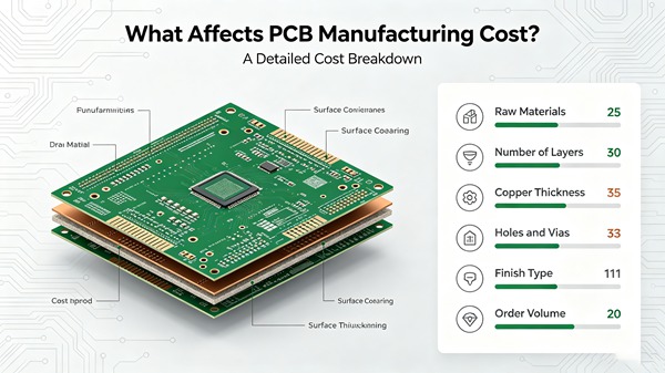
Table des matières
Le nombre de couches est l'un des principaux facteurs de coût
L'augmentation du nombre de couches d'un circuit imprimé entraîne généralement une hausse des coûts de fabrication.
La fabrication d'un circuit imprimé à deux couches suit un processus relativement simple. Un circuit imprimé multicouche nécessite en outre :
- Imagerie des couches internes
- Lamination
- Forage
- Placage
- L'inspection
- Contrôle des inscriptions
Par exemple, passer d'un circuit imprimé à 4 couches à un circuit imprimé à 8 couches ne se résume pas simplement à ajouter quatre couches de cuivre. Les étapes supplémentaires de stratification et de traitement allongent également le temps de fabrication et accroissent la complexité de la production.
À lire également : Fabrication de circuits imprimés multicouches
Toutefois, la réduction du nombre de couches ne doit pas être considérée comme une mesure permettant automatiquement de réaliser des économies.
Une réduction du nombre de couches peut nécessiter :
- Un acheminement plus complexe
- Dimensions de la planche plus grandes
- Plus de vias
- Autres problèmes liés à l'intégrité du signal
La cible correcte est la nombre minimal de couches permettant de satisfaire aux exigences électriques et mécaniques.
Le matériau utilisé pour les circuits imprimés a une incidence directe sur le coût
Le FR-4 standard est généralement plus économique que les matériaux spécialisés.
Selon l'application, les ingénieurs peuvent avoir besoin :
- FR-4 standard
- FR-4 à haute Tg
- Stratifiés à faibles pertes
- Matériaux à base de PTFE
- Matériaux haute fréquence
- Substrats à noyau métallique
Le choix des matériaux a une incidence tant sur le prix des matières premières que sur le processus de fabrication.
Pour les conceptions à haute vitesse ou RF, le choix d'un stratifié moins cher dans le seul but de réduire le coût du circuit imprimé peut entraîner des problèmes liés à :
- Perte diélectrique
- Stabilité de l'impédance
- Performances thermiques
- Intégrité du signal
À lire également : Choix des matériaux pour les circuits imprimés haute fréquence
Le choix du matériau doit donc se faire en fonction des exigences électriques et environnementales réelles, plutôt qu’en se basant uniquement sur le prix.
La taille des circuits imprimés et l'utilisation des panneaux influent sur l'efficacité de la fabrication
Les panneaux de plus grandes dimensions nécessitent davantage de stratifié et occupent plus d'espace de production.
Cependant, la taille de la planche n'est pas le seul critère à prendre en compte.
Les fabricants disposent généralement plusieurs circuits imprimés sur un panneau de production plus grand.
Une meilleure utilisation des panneaux peut permettre de réduire :
- Gaspillage de matériaux
- Frais généraux de production
- Coût par carte
C'est pourquoi une légère modification des dimensions des cartes peut parfois avoir un impact étonnamment important sur le coût unitaire, lorsqu'elle permet de disposer plus efficacement un plus grand nombre de cartes sur un panneau de production.
À lire également : Consignes relatives à la panélisation des circuits imprimés
La variation du cours du cuivre modifie les exigences de fabrication
Les conceptions de circuits imprimés standard utilisent souvent du cuivre de 1 oz, mais certaines applications nécessitent :
- 2 oz de cuivre
- 3 oz de cuivre
- 4 oz de cuivre
- Structures en cuivre massif
L'augmentation de l'épaisseur du cuivre entraîne une augmentation des besoins en matière de matériaux et de traitement.
Le cuivre épais peut également nécessiter des ajustements au niveau :
- Gravure
- Placage
- Géométrie de tracé
- Gestion thermique
Dans le domaine de l'électronique de puissance, toutefois, le surcoût peut se justifier au regard des exigences électriques et thermiques.
À lire également : Conception de circuits imprimés électroniques de puissance pour véhicules électriques
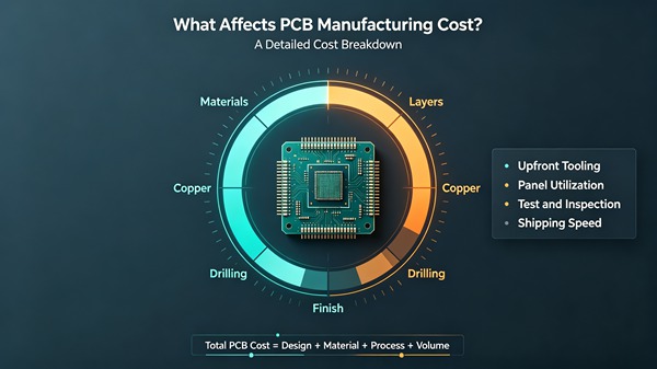
Le diamètre du foret et le nombre de trous ont leur importance
Le perçage constitue un autre facteur important dans les coûts de fabrication.
Une carte comportant des centaines de trous traversants standard est généralement plus facile à fabriquer qu'une carte nécessitant un grand nombre de trous très petits.
Le coût peut augmenter lorsqu'une conception nécessite :
- Très petites perceuses mécaniques
- Microvias laser
- Vias aveugles
- Vias enterrés
- Perçage en retrait
- Trous à rapport d'aspect élevé
Le nombre de trous influe également sur la durée du forage et le débit de production.
Les structures HDI accroissent la complexité
La technologie HDI peut augmenter considérablement le coût de fabrication des circuits imprimés, car elle peut nécessiter :
- Perçage au laser
- Laminage séquentiel
- Remplissage des microvias
- Placage supplémentaire
- Un contrôle plus strict des immatriculations
Le HDI doit donc être utilisé lorsqu'il apporte un réel avantage en termes de conception, par exemple :
- Taille de carte réduite
- Routage de circuits imprimés BGA à pas fin
- Une densité de routage plus élevée
- Réduction du nombre de couches
À lire également : Fabrication de circuits imprimés HDI
Le recours à la technologie HDI simplement parce que la conception le permet peut entraîner une augmentation inutile des coûts de fabrication.
La finition de surface influe sur le prix des circuits imprimés
Les finitions de surface les plus courantes sont les suivantes :
- HASL
- HASL sans plomb
- ENIG
- Argent d'immersion
- Étain d'immersion
- OSP
Le procédé ENIG coûte généralement plus cher que le procédé HASL classique en raison des étapes de traitement supplémentaires et des besoins en matériaux.
Toutefois, le traitement de surface doit être choisi en fonction des exigences en matière d'assemblage et de fiabilité.
Par exemple, les composants à pas fin et certaines applications de contact peuvent tirer parti d'une finition de surface plus lisse.
Opter pour la finition la moins chère n'est pas forcément la décision la plus économique si cela entraîne par la suite des problèmes de montage.
Exigences relatives à l'épaisseur et aux tolérances des circuits imprimés
Les épaisseurs standard des panneaux sont généralement plus économiques que les spécifications atypiques.
Des frais supplémentaires peuvent résulter :
- Épaisseur hors norme
- Tolérance d'épaisseur très stricte
- Épaisseur diélectrique spécifique
- Exigences en matière d'impédance complexe
Si une conception ne nécessite pas d'épaisseur particulière, le recours à une structure standard peut simplifier la production.
Des règles de conception strictes font augmenter les coûts de fabrication
La fabrication devient plus difficile lorsqu'une conception atteint les limites du processus du fournisseur.
On peut citer par exemple :
- Pistes extrêmement étroites
- Espacement très réduit
- Petits anneaux
- Petits trous mécaniques
- Tolérances d'alignement très strictes
Ces exigences pourraient augmenter :
- Difficulté de production
- Risque de mise au rebut
- Exigences en matière d'inspection
- Délai de fabrication
C'est pourquoi il convient de prendre en compte les aspects liés à la fabrication (DFM) avant que la conception ne soit validée pour la production.
L'impédance contrôlée peut avoir une incidence sur le coût des circuits imprimés
Le fait d'avoir une impédance contrôlée ne rend pas nécessairement un circuit imprimé plus cher.
L'impact sur les coûts dépend de la manière dont les exigences en matière d'impédance influent sur la construction.
Par exemple, les ingénieurs peuvent être amenés à préciser :
- Épaisseur diélectrique spécifique
- Épaisseur de cuivre contrôlée
- Largeur précise des pistes
- Stratifié spécialisé
Des tolérances d'impédance plus strictes peuvent également nécessiter des essais supplémentaires et un contrôle accru des processus.
L'évolution du volume de production influe sur le coût unitaire
La fabrication de circuits imprimés devient généralement plus rentable à mesure que le volume de production augmente.
Une petite commande de prototypes peut entraîner des coûts relativement élevés liés à :
- Préparation technique
- Outillage
- Configuration
- Manutention
Ces coûts sont répartis sur un plus grand nombre de circuits imprimés lorsque les séries de production sont plus importantes.
Cependant, augmenter les quantités dans le seul but d'obtenir un prix unitaire plus bas n'est pas toujours judicieux sur le plan financier.
Pour les projets en phase de démarrage, il est souvent préférable de produire une petite quantité, de valider la conception, puis d'augmenter le volume une fois que celle-ci est stabilisée.
Les exigences en matière de tests peuvent faire augmenter les coûts
Les essais électriques de base sur les circuits imprimés diffèrent des essais avancés de qualification de fiabilité.
D'autres examens peuvent être réalisés, notamment :
- Test par sonde mobile
- Inspection optique automatisée
- inspection par rayons X
- Analyse transversale
- Cyclage thermique
- Test d'impédance
Le niveau d'inspection approprié dépend de l'application.
Une simple carte prototype ne nécessite pas forcément le même processus de qualification qu'une carte de commande automobile.
Comment réduire les coûts de fabrication des circuits imprimés sans compromettre la qualité
1. Utiliser des matériaux standard dans la mesure du possible
Si le FR-4 standard répond aux exigences électriques et thermiques, il n'y a peut-être pas lieu de choisir un matériau plus coûteux.
2. Évitez d'utiliser un nombre excessif de couches
Vérifiez l'empilement et le tracé avant d'augmenter le nombre de couches.
3. Utiliser des épaisseurs de panneaux standard
Les constructions standard sont généralement plus faciles à mettre en œuvre pour les fabricants.
4. Évitez les règles de conception extrêmes
Évitez de concevoir des produits dont les dimensions se rapprochent inutilement de la capacité minimale de fabrication.
5. Optimiser la panélisation
Les dimensions des panneaux doivent être examinées en tenant compte du taux d'utilisation des panneaux de production.
6. Choisir la finition de surface en fonction de l'application
Ne choisissez pas systématiquement la finition la plus chère.
7. Privilégiez le coût total plutôt que le prix unitaire
Le devis le moins cher pour un circuit imprimé ne correspond pas forcément au coût total le plus bas.
Une carte de mauvaise qualité peut entraîner :
- Révision de l'assemblage
- Temps de débogage
- Ferraille
- Retards de livraison
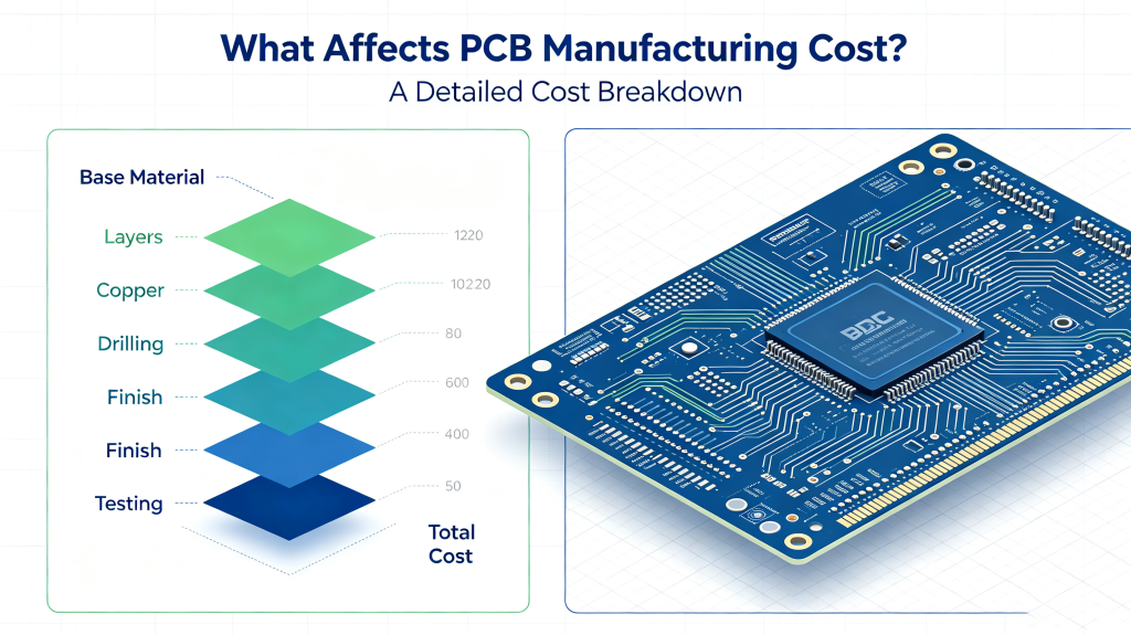
Guide pratique : comment examiner un devis de circuit imprimé
Lorsque vous comparez des devis pour des circuits imprimés, vérifiez les points suivants.
Étape 1 : Vérifier les spécifications de base
Vérifier :
- Nombre de couches
- Dimensions de la planche
- Épaisseur
- Poids du cuivre
- Matériau
Étape 2 : Vérifier les processus spéciaux
Rechercher :
- Vias aveugles
- Vias enterrés
- Microvias
- Perçage en retrait
- Cuivre épais
- Impédance contrôlée
Étape 3 : Comparer les finitions de surface
Assurez-vous que tous les fournisseurs proposent la même finition dans leurs devis.
Étape 4 : Vérifier les exigences en matière de tests
Vérifiez si le devis comprend :
- Essais électriques
- AOI
- Test d'impédance
- Autres contrôles demandés
Étape 5 : Comparer les délais de livraison
Un prix plus bas peut ne pas être avantageux s'il entraîne des retards inacceptables.
Étape 6 : Comparer le coût total
Réfléchissez à ceci :
Prix du circuit imprimé + outillage + tests + expédition + éventuelles retouches
plutôt que de se contenter de comparer le prix unitaire des cartes.
Exemple de coût d'un circuit imprimé
Considérons deux panneaux ayant les mêmes dimensions extérieures.
Tableau A
- 4 couches
- FR-4 standard
- 1 once de cuivre
- Trous traversants standard
- HASL
- Tolérances standard
Tableau B
- 8 couches
- Matériau à haute Tg
- 2 oz de cuivre
- Microvias
- Impédance contrôlée
- ENIG
- Tolérances dimensionnelles très strictes
Même si ces cartes peuvent sembler similaires à première vue, la carte B nécessite un traitement nettement plus complexe et un contrôle des processus plus rigoureux.
Cela montre pourquoi Le prix d'un circuit imprimé ne peut pas être estimé avec précision en se basant uniquement sur la taille de la carte..
FAQ
R : Le nombre de couches, le matériau, la taille du circuit imprimé, l'épaisseur de la couche de cuivre, la complexité de fabrication et le volume de production comptent parmi les facteurs les plus importants.
R : En général, oui, même si l'ajout de couches supplémentaires peut parfois simplifier le routage et réduire d'autres contraintes de fabrication.
R : En général, oui. Le procédé ENIG nécessite des traitements de finition de surface et des matériaux supplémentaires.
R : Commencez par examiner le nombre de couches, le choix des matériaux, les dimensions des cartes, l'utilisation des panneaux, les exigences en matière de perçage et les restrictions de tolérance superflues.
R : Pas forcément. Les problèmes de qualité, les retards de livraison et les difficultés de montage peuvent faire en sorte qu'un prix initial bas revienne finalement plus cher au final.
Conclusion
Le coût de fabrication des circuits imprimés dépend de l'interaction entre la conception, les matériaux, les procédés de fabrication, les exigences en matière d'essais et le volume de production.
Le moyen le plus efficace de réduire les coûts ne consiste pas simplement à trouver le devis le moins cher. Les ingénieurs doivent plutôt repérer les complexités superflues et optimiser la conception avant la production.
Une stratégie concrète de réduction des coûts consiste à :
- Utilisez des matériaux adaptés
- Optimiser le nombre de couches
- Simplifier les éléments de fabrication superflus
- Optimiser l'utilisation des panneaux
- Utilisez des tolérances réalistes
- Adapter les exigences en matière d'essais à l'application
Cette approche permet de réduire les coûts de fabrication des circuits imprimés tout en respectant les exigences électriques, mécaniques et de fiabilité du produit final.
 FR
FR  EN
EN  PT
PT  AR
AR  DE
DE  ES
ES