Wenn Ingenieure ein Angebot für eine Leiterplatte anfordern, kann der Endpreis manchmal erheblich von ihren ursprünglichen Erwartungen abweichen.
Zwei Platinen mit ähnlichen Abmessungen können völlig unterschiedliche Herstellungskosten aufweisen, da sich ihre inneren Strukturen, Materialien, Toleranzen und Produktionsanforderungen unterscheiden.
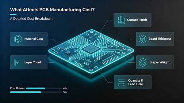
Zu den wichtigsten Kostenfaktoren zählen in der Regel:
- Anzahl der Schichten
- Abmessungen der Platte
- Auswahl des Materials
- Kupfergewicht
- Anzahl der Bohrlöcher und Bohranforderungen
- Mindestleiterbahnbreite und -abstand
- Oberflächengüte
- PCB-Dicke
- Spezielle Fertigungsverfahren
- Produktionsmenge
Wenn man diese Faktoren versteht, lässt sich leichter Angebote vergleichen und erkennen, wo tatsächlich Kosten eingespart werden können.
Inhaltsübersicht
Die Anzahl der Schichten ist einer der größten Kostenfaktoren
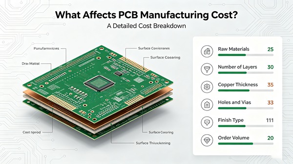
Eine Erhöhung der Anzahl der Leiterplattenlagen führt in der Regel zu höheren Herstellungskosten.
Die Fertigung einer zweilagigen Leiterplatte erfolgt in relativ einfachen Schritten. Bei einer mehrlagigen Leiterplatte sind zusätzlich erforderlich:
- Bildgebung der inneren Schichten
- Kaschierung
- Bohren
- Beschichtung
- Inspektion
- Registrierungskontrolle
So ist beispielsweise der Wechsel von einer 4-lagigen Leiterplatte zu einer 8-lagigen Leiterplatte nicht einfach nur eine Frage des Hinzufügens von vier Kupferschichten. Die zusätzlichen Laminier- und Verarbeitungsschritte erhöhen zudem die Fertigungszeit und die Komplexität der Produktion.
Siehe auch: Herstellung von Mehrschicht-Leiterplatten
Die Reduzierung der Schichtenanzahl sollte jedoch nicht als automatische Kosteneinsparungsmaßnahme betrachtet werden.
Eine geringere Anzahl von Schichten kann Folgendes erfordern:
- Kompliziertere Routenführung
- Größere Plattenabmessungen
- Weitere Durchkontaktierungen
- Weitere Beeinträchtigungen der Signalintegrität
Das richtige Ziel ist das geringste praktikable Schichtenanzahl, die die elektrischen und mechanischen Anforderungen erfüllt.
Das Leiterplattenmaterial wirkt sich direkt auf die Kosten aus
Standard-FR-4 ist in der Regel kostengünstiger als Spezialmaterialien.
Je nach Anwendungsfall benötigen Ingenieure möglicherweise:
- Standard FR-4
- FR-4 mit hoher Glasübergangstemperatur
- Verlustarme Laminate
- Materialien auf PTFE-Basis
- Hochfrequente Materialien
- Metallkern-Substrate
Die Materialauswahl wirkt sich sowohl auf den Rohstoffpreis als auch auf den Herstellungsprozess aus.
Bei Hochgeschwindigkeits- oder HF-Designs kann die Wahl eines günstigeren Laminats – allein zur Senkung der Leiterplattenkosten – zu folgenden Problemen führen:
- Dielektrischer Verlust
- Impedanzstabilität
- Wärmeleistung
- Signalintegrität
Siehe auch: Materialauswahl für Hochfrequenz-Leiterplatten
Das Material sollte daher eher anhand der tatsächlichen elektrischen und umgebungsbezogenen Anforderungen als allein nach dem Preis ausgewählt werden.
Plattengröße und Plattenauslastung beeinflussen die Fertigungseffizienz
Größere Platten verbrauchen mehr Laminatmaterial und beanspruchen mehr Produktionsfläche.
Allerdings ist die Größe der Platine nicht der einzige zu berücksichtigende Faktor.
Hersteller ordnen in der Regel mehrere Leiterplatten auf einer größeren Produktionsplatte an.
Eine bessere Auslastung der Panels kann Folgendes reduzieren:
- Materialverschwendung
- Produktionsgemeinkosten
- Kosten pro Platine
Aus diesem Grund kann eine geringfügige Änderung der Leiterplattenabmessungen mitunter überraschend große Auswirkungen auf die Stückkosten haben, wenn dadurch mehr Leiterplatten effizient auf einer Fertigungsplatte untergebracht werden können.
Siehe auch: Richtlinien zur Panelisierung von Leiterplatten
Das Kupfergewicht beeinflusst die Fertigungsanforderungen
Bei Standard-Leiterplattenentwürfen wird häufig 1 oz Kupfer verwendet, doch für manche Anwendungen sind folgende Anforderungen zu beachten:
- 2 Unzen Kupfer
- 3 oz Kupfer
- 4 oz Kupfer
- Schwere Kupferkonstruktionen
Mit zunehmender Kupferdicke steigen die Anforderungen an Material und Verarbeitung.
Bei dickwandigem Kupfer können außerdem Anpassungen erforderlich sein an:
- Ätzen
- Beschichtung
- Konturgeometrie
- Thermisches Management
Im Bereich der Leistungselektronik können die zusätzlichen Kosten jedoch durch die elektrischen und thermischen Anforderungen gerechtfertigt sein.
Siehe auch: Leistungselektronik-Leiterplattenentwurf für Elektrofahrzeuge
Bohrergröße und Anzahl der Bohrlöcher sind entscheidend
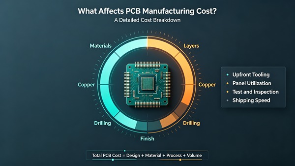
Das Bohren ist ein weiterer wichtiger Faktor bei den Fertigungskosten.
Eine Leiterplatte mit Hunderten von Standard-Durchkontaktierungen lässt sich in der Regel leichter herstellen als eine, die eine große Anzahl sehr kleiner Löcher erfordert.
Die Kosten können steigen, wenn ein Entwurf Folgendes erfordert:
- Sehr kleine mechanische Bohrmaschinen
- Laser-Mikrovias
- Blinde Durchkontaktierungen
- Vergrabene Durchkontaktierungen
- Rückbohren
- Löcher mit hohem Seitenverhältnis
Die Anzahl der Bohrlöcher wirkt sich ebenfalls auf die Bohrzeit und den Produktionsdurchsatz aus.
HDI-Strukturen erhöhen die Komplexität
Die HDI-Technologie kann die Herstellungskosten für Leiterplatten erheblich erhöhen, da sie unter Umständen Folgendes erfordert:
- Laserbohren
- Sequentielles Laminieren
- Füllung von Microvias
- Zusätzliche Beschichtung
- Strengere Zulassungskontrolle
HDI sollte daher dort eingesetzt werden, wo es einen echten Konstruktionsvorteil bietet, beispielsweise:
- Kleinere Plattengröße
- BGA-Verlegung mit engem Rasterabstand
- Höhere Routing-Dichte
- Reduzierte Schichtenanzahl
Siehe auch: HDI PCB-Herstellung
Der Einsatz von HDI allein deshalb, weil das Design dies zulässt, kann die Herstellungskosten unnötig in die Höhe treiben.
Die Oberflächenbeschaffenheit beeinflusst den Preis der Leiterplatte
Übliche Oberflächenbehandlungen sind:
- HASL
- Bleifreies HASL
- ENIG
- Eintauchen Silber
- Tauchbad
- OSP
ENIG ist aufgrund der zusätzlichen Verarbeitungsschritte und des höheren Materialbedarfs in der Regel teurer als herkömmliches HASL.
Die Oberflächenbeschaffenheit sollte jedoch entsprechend den Anforderungen an die Montage und die Zuverlässigkeit ausgewählt werden.
So können beispielsweise Bauteile mit engem Rastermaß und bestimmte Kontaktanwendungen von einer glatteren Oberflächenbeschaffenheit profitieren.
Die Wahl der günstigsten Oberflächenbehandlung ist nicht unbedingt die wirtschaftlichste Entscheidung, wenn dadurch später Montageprobleme entstehen.
Anforderungen an die Dicke und Toleranz von Leiterplatten
Standard-Plattenstärken sind in der Regel kostengünstiger als Sonderausführungen.
Zusätzliche Kosten können entstehen durch:
- Abweichende Dicke
- Enge Dickentoleranz
- Spezielle Dielektrikumsdicke
- Anforderungen an die komplexe Impedanz
Wenn eine Konstruktion keine ungewöhnliche Dicke erfordert, kann die Verwendung einer Standardmaterialkonstruktion die Fertigung vereinfachen.
Strenge Konstruktionsvorschriften erhöhen die Herstellungskosten
Die Fertigung wird schwieriger, wenn ein Entwurf an die Prozessgrenzen des Lieferanten stößt.
Beispiele hierfür sind:
- Extrem schmale Leiterbahnen
- Sehr geringer Abstand
- Winzige ringförmige Ringe
- Kleine mechanische Bohrungen
- Enge Passgenauigkeitstoleranzen
Diese Anforderungen können sich erhöhen:
- Produktionsschwierigkeiten
- Schrottrisiko
- Prüfvorschriften
- Herstellungszeit
Aus diesem Grund sollte DFM berücksichtigt werden, bevor der Entwurf für die Produktion freigegeben wird.
Eine kontrollierte Impedanz kann sich auf die Kosten von Leiterplatten auswirken
Eine kontrollierte Impedanz allein macht eine Leiterplatte nicht unbedingt teuer.
Die Auswirkungen auf die Kosten hängen davon ab, inwieweit sich die Impedanzanforderung auf die Bauweise auswirkt.
Beispielsweise müssen Ingenieure möglicherweise Folgendes festlegen:
- Spezifische Dielektrikumsdicke
- Kontrollierte Kupferdicke
- Präzise Leiterbahnbreite
- Spezial-Laminat
Strengere Impedanztoleranzen können zudem zusätzliche Prüfungen und Prozesskontrollen erforderlich machen.
Das Produktionsvolumen beeinflusst die Stückkosten
Die Leiterplattenfertigung wird in der Regel mit steigender Produktionsmenge wirtschaftlicher.
Ein kleiner Prototypenauftrag kann relativ hohe Kosten verursachen, die sich aus folgenden Faktoren ergeben:
- Technische Vorbereitung
- Werkzeuge
- Einrichtung
- Materialtransport
Bei größeren Produktionsmengen verteilen sich diese Kosten auf eine größere Anzahl von Leiterplatten.
Eine reine Steigerung der Menge, nur um einen niedrigeren Stückpreis zu erzielen, ist jedoch nicht immer wirtschaftlich sinnvoll.
Bei Projekten in der Anfangsphase ist es oft besser, zunächst eine kleinere Stückzahl zu fertigen, das Design zu validieren und erst dann, wenn das Design stabil ist, die Stückzahl zu erhöhen.
Prüfanforderungen können die Kosten erhöhen
Die grundlegende elektrische Prüfung von Leiterplatten unterscheidet sich von der fortgeschrittenen Zuverlässigkeitsprüfung.
Weitere Untersuchungen können Folgendes umfassen:
- Flying-Probe-Test
- Automatisierte optische Inspektion
- Röntgenprüfung
- Querschnittsanalyse
- Thermisches Zyklieren
- Impedanzprüfung
Der richtige Prüfumfang hängt von der jeweiligen Anwendung ab.
Eine einfache Prototypenplatine erfordert nicht unbedingt denselben Qualifizierungsprozess wie eine Steuerplatine für Kraftfahrzeuge.
So senken Sie die Kosten für die Leiterplattenfertigung, ohne Abstriche bei der Qualität zu machen
1. Verwenden Sie nach Möglichkeit Standardmaterialien
Wenn Standard-FR-4 die elektrischen und thermischen Anforderungen erfüllt, gibt es möglicherweise kaum einen Grund, ein teureres Material zu spezifizieren.
2. Vermeiden Sie eine unnötig hohe Anzahl von Ebenen
Überprüfen Sie den Schichtaufbau und die Leiterbahnführung, bevor Sie die Anzahl der Schichten erhöhen.
3. Verwenden Sie Standard-Plattenstärken
Standardkonstruktionen lassen sich von den Herstellern in der Regel leichter verarbeiten.
4. Vermeiden Sie extreme Designregeln
Entwerfen Sie nicht unnötig nahe an der minimalen Fertigungsfähigkeit.
5. Optimierung der Plattenaufteilung
Die Abmessungen der Platten sollten im Zusammenhang mit der Ausnutzung der Produktionsplatten überprüft werden.
6. Wählen Sie die Oberflächenbeschaffenheit entsprechend der Anwendung aus
Entscheiden Sie sich nicht automatisch für die teuerste Ausführung.
7. Berücksichtigen Sie die Gesamtkosten statt des Stückpreises
Das günstigste Angebot für Leiterplatten bedeutet nicht zwangsläufig die niedrigsten Gesamtkosten.
Ein minderwertiges Board kann Folgendes verstärken:
- Nachbearbeitung der Montage
- Debugging-Zeit
- Schrott
- Produktverzögerungen
Anleitung: Ein Angebot für eine Leiterplatte prüfen
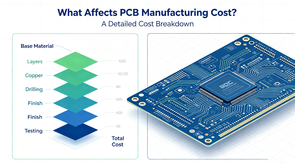
Achten Sie beim Vergleich von Angeboten für Leiterplatten auf die folgenden Punkte.
Schritt 1: Bestätigen Sie die grundlegenden Spezifikationen
Überprüfen:
- Anzahl der Schichten
- Abmessungen der Platte
- Dicke
- Kupfergewicht
- Material
Schritt 2: Spezielle Prozesse überprüfen
Suchen Sie nach:
- Blinde Durchkontaktierungen
- Vergrabene Durchkontaktierungen
- Mikrobohrungen
- Rückbohren
- Schweres Kupfer
- Kontrollierte Impedanz
Schritt 3: Oberflächenbeschaffenheit vergleichen
Stellen Sie sicher, dass alle Lieferanten dieselbe Oberflächenausführung anbieten.
Schritt 4: Prüfungsanforderungen prüfen
Bitte bestätigen Sie, ob das Angebot Folgendes umfasst:
- Elektrische Prüfung
- AOI
- Impedanzprüfung
- Sonstige beantragte Inspektionen
Schritt 5: Lieferzeiten vergleichen
Ein niedrigerer Preis ist möglicherweise nicht sinnvoll, wenn er zu inakzeptablen Verzögerungen führt.
Schritt 6: Vergleichen Sie die Gesamtkosten
Bedenken Sie Folgendes:
Leiterplattenpreis + Werkzeugkosten + Prüfung + Versand + eventuelle Nacharbeiten
anstatt nur den Stückpreis der Platine zu vergleichen.
Beispiel für Leiterplattenkosten
Betrachten wir zwei Platten mit denselben Außenabmessungen.
Tafel A
- 4 Schichten
- Standard FR-4
- 1 Unze Kupfer
- Standard-Durchgangsbohrungen
- HASL
- Standardtoleranzen
Tafel B
- 8 Schichten
- Material mit hoher Glasübergangstemperatur
- 2 Unzen Kupfer
- Mikrobohrungen
- Kontrollierte Impedanz
- ENIG
- Enge Maßtoleranzen
Auch wenn die Platinen von außen ähnlich aussehen mögen, erfordert Platine B einen deutlich höheren Bearbeitungsaufwand und eine strengere Prozesskontrolle.
Dies verdeutlicht, warum Der Preis einer Leiterplatte lässt sich nicht allein anhand der Plattengröße genau abschätzen.
FAQ
A: Zu den wichtigsten Faktoren zählen die Anzahl der Schichten, das Material, die Leiterplattengröße, die Kupferdicke, die Komplexität der Fertigung und die Produktionsmenge.
A: Im Allgemeinen ja, obwohl zusätzliche Schichten manchmal die Verdrahtung vereinfachen und andere Fertigungsanforderungen verringern können.
A: In der Regel ja. ENIG erfordert zusätzliche Oberflächenbehandlungsverfahren und Materialien.
A: Überprüfen Sie zunächst die Anzahl der Schichten, die Materialauswahl, die Plattenabmessungen, die Plattenausnutzung, die Bohrungsanforderungen und unnötige Toleranzbeschränkungen.
A: Nicht unbedingt. Qualitätsprobleme, Lieferverzögerungen und Montageprobleme können dazu führen, dass ein niedriger Anschaffungspreis insgesamt teurer wird.
Schlussfolgerung
Das Zusammenspiel von Design, Materialien, Fertigungsverfahren, Prüfanforderungen und Produktionsvolumen bestimmt die Herstellungskosten von Leiterplatten.
Der effektivste Weg, Kosten zu senken, besteht nicht einfach darin, das günstigste Angebot zu finden. Vielmehr sollten Ingenieure unnötige Komplexität aufdecken und die Konstruktion vor der Produktion optimieren.
Eine praktische Strategie zur Kostensenkung besteht darin:
- Verwenden Sie geeignete Materialien
- Optimieren Sie die Anzahl der Schichten
- Unnötige Konstruktionsmerkmale vereinfachen
- Die Auslastung der Platten verbessern
- Verwenden Sie realistische Toleranzen
- Anforderungen an die Prüfung an die jeweilige Anwendung anpassen
Dieser Ansatz kann die Herstellungskosten für Leiterplatten senken und gleichzeitig die elektrischen, mechanischen und Zuverlässigkeitsanforderungen des Endprodukts erfüllen.
 DE
DE  EN
EN  PT
PT  AR
AR  FR
FR  ES
ES