When engineers request a PCB quotation, the final price can sometimes be very different from what they initially expect.
Two boards with similar dimensions may have completely different manufacturing costs because their internal structures, materials, tolerances, and production requirements are different.
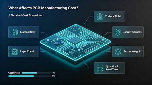
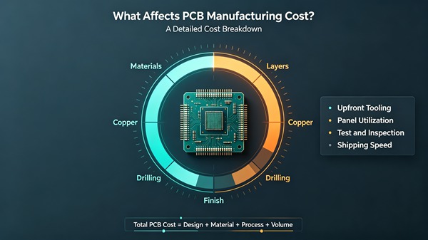
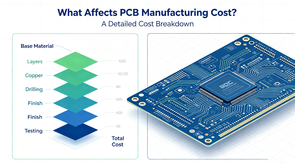
The main cost drivers usually include:
- Layer count
- Board dimensions
- Material selection
- Copper weight
- Hole count and drilling requirements
- Minimum trace and spacing
- Surface finish
- PCB thickness
- Special fabrication processes
- Production quantity
Understanding these factors makes it easier to compare quotations and identify where cost can actually be reduced.
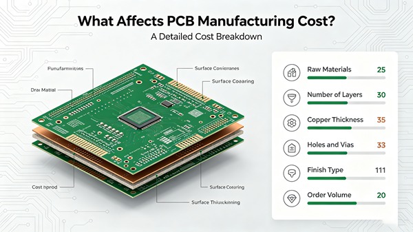
Table of Contents
Layer Count Is One of the Biggest Cost Drivers
Increasing the number of PCB layers usually increases manufacturing cost.
A two-layer PCB has a relatively simple fabrication sequence. A multilayer PCB requires additional:
- Inner-layer imaging
- Lamination
- Drilling
- Plating
- Inspection
- Registration control
For example, moving from a 4-layer board to an 8-layer board is not simply a matter of adding four copper layers. The additional lamination and processing steps also increase manufacturing time and production complexity.
Related: Multilayer PCB Manufacturing
However, reducing layer count should not be treated as an automatic cost-saving measure.
A lower layer count may require:
- More complicated routing
- Larger board dimensions
- More vias
- Additional signal integrity compromises
The correct target is the lowest practical layer count that meets the electrical and mechanical requirements.
PCB Material Has a Direct Impact on Cost
Standard FR-4 is generally more economical than specialized materials.
Depending on the application, engineers may need:
- Standard FR-4
- High-Tg FR-4
- Low-loss laminates
- PTFE-based materials
- High-frequency materials
- Metal-core substrates
Material selection affects both the raw material price and manufacturing process.
For high-speed or RF designs, choosing a cheaper laminate simply to reduce PCB cost may create problems with:
- Dielectric loss
- Impedance stability
- Thermal performance
- Signal integrity
The material should therefore be selected according to the actual electrical and environmental requirements rather than price alone.
Board Size and Panel Utilization Affect Manufacturing Efficiency
Larger boards consume more laminate material and occupy more production area.
However, board size is not the only consideration.
Manufacturers normally arrange multiple PCBs onto a larger production panel.
Better panel utilization can reduce:
- Material waste
- Production overhead
- Cost per board
For this reason, a small change in board dimensions can sometimes have a surprisingly large impact on unit cost when it allows more boards to fit efficiently onto a production panel.
Related: PCB Panelization Guidelines
Copper Weight Changes the Manufacturing Requirement
Standard PCB designs often use 1 oz copper, but some applications require:
- 2 oz copper
- 3 oz copper
- 4 oz copper
- Heavy copper structures
Increasing copper thickness increases material and processing requirements.
Heavy copper can also require adjustments to:
- Etching
- Plating
- Trace geometry
- Thermal management
For power electronics, however, the additional cost may be justified by the electrical and thermal requirements.
Related: Power Electronics PCB Design for EV
Drill Size and Hole Quantity Matter
Drilling is another important manufacturing cost factor.
A board containing hundreds of standard through-holes is generally easier to manufacture than one requiring large numbers of very small holes.
Cost can increase when a design requires:
- Very small mechanical drills
- Laser microvias
- Blind vias
- Buried vias
- Backdrilling
- High aspect-ratio holes
The number of holes also affects drilling time and production throughput.
HDI Structures Increase Complexity
HDI technology can significantly increase PCB manufacturing cost because it may require:
- Laser drilling
- Sequential lamination
- Microvia filling
- Additional plating
- Tighter registration control
HDI should therefore be used where it provides a real design benefit, such as:
- Smaller board size
- Fine-pitch BGA routing
- Higher routing density
- Reduced layer count
Related: HDI PCB Manufacturing
Using HDI simply because the design can support it may unnecessarily increase manufacturing cost.
Surface Finish Affects PCB Price
Common surface finishes include:
- HASL
- Lead-free HASL
- ENIG
- Immersion silver
- Immersion tin
- OSP
ENIG generally costs more than conventional HASL because of its additional processing steps and material requirements.
However, surface finish should be selected according to the assembly and reliability requirements.
For example, fine-pitch components and certain contact applications may benefit from a flatter surface finish.
Choosing the cheapest finish is not necessarily the most economical decision if it creates assembly problems later.
PCB Thickness and Tolerance Requirements
Standard board thicknesses are usually more economical than unusual specifications.
Additional cost can result from:
- Non-standard thickness
- Tight thickness tolerance
- Special dielectric thickness
- Complex impedance requirements
If a design does not require an unusual thickness, using a standard material construction can simplify production.
Tight Design Rules Increase Manufacturing Cost
Manufacturing becomes more difficult when a design approaches the supplier’s process limits.
Examples include:
- Extremely narrow traces
- Very small spacing
- Tiny annular rings
- Small mechanical holes
- Tight registration tolerances
These requirements may increase:
- Production difficulty
- Scrap risk
- Inspection requirements
- Manufacturing time
This is why DFM should be considered before the design is released for production.
Controlled Impedance Can Affect PCB Cost
Controlled impedance itself does not necessarily make a PCB expensive.
The cost impact depends on how the impedance requirement affects the construction.
For example, engineers may need to specify:
- Specific dielectric thickness
- Controlled copper thickness
- Precise trace width
- Specialized laminate
More demanding impedance tolerances may also require additional testing and process control.
Production Volume Changes the Unit Cost
PCB manufacturing generally becomes more economical as production quantity increases.
A small prototype order may carry relatively high costs from:
- Engineering preparation
- Tooling
- Setup
- Material handling
These costs are distributed across more boards during larger production runs.
However, increasing quantity solely to obtain a lower unit price is not always financially sensible.
For early-stage projects, it is often better to manufacture a smaller quantity, validate the design, and then increase volume after the design is stable.
Testing Requirements Can Increase Cost
Basic PCB electrical testing is different from advanced reliability qualification.
Additional testing may include:
- Flying probe testing
- Automated optical inspection
- X-ray inspection
- Cross-section analysis
- Thermal cycling
- Impedance testing
The right inspection level depends on the application.
A simple prototype board does not necessarily require the same qualification process as an automotive control board.
How to Reduce PCB Manufacturing Cost Without Sacrificing Quality
1. Use Standard Materials Where Possible
If standard FR-4 meets the electrical and thermal requirements, there may be little reason to specify a more expensive material.
2. Avoid Unnecessary Layer Count
Review the stackup and routing before increasing layer count.
3. Use Standard Board Thicknesses
Standard constructions are usually easier for manufacturers to process.
4. Avoid Extreme Design Rules
Do not design unnecessarily close to the minimum manufacturing capability.
5. Optimize Panelization
Board dimensions should be reviewed together with production panel utilization.
6. Select Surface Finish According to Application
Do not automatically choose the most expensive finish.
7. Consider Total Cost Instead of Unit Price
The cheapest PCB quotation is not necessarily the lowest total cost.
A poor-quality board can increase:
- Assembly rework
- Debugging time
- Scrap
- Product delays
How-To: Review a PCB Quotation
When comparing PCB quotations, check the following items.
Step 1: Confirm the Basic Specification
Check:
- Layer count
- Board dimensions
- Thickness
- Copper weight
- Material
Step 2: Check Special Processes
Look for:
- Blind vias
- Buried vias
- Microvias
- Backdrilling
- Heavy copper
- Controlled impedance
Step 3: Compare Surface Finish
Make sure all suppliers are quoting the same finish.
Step 4: Check Testing Requirements
Confirm whether the quotation includes:
- Electrical testing
- AOI
- Impedance testing
- Other requested inspections
Step 5: Compare Lead Time
A lower price may not be useful if it creates unacceptable delays.
Step 6: Compare the Complete Cost
Consider:
PCB price + tooling + testing + shipping + potential rework
rather than comparing the board unit price alone.
PCB Cost Example
Consider two boards with the same external dimensions.
Board A
- 4 layers
- Standard FR-4
- 1 oz copper
- Standard through-holes
- HASL
- Standard tolerances
Board B
- 8 layers
- High-Tg material
- 2 oz copper
- Microvias
- Controlled impedance
- ENIG
- Tight dimensional tolerances
Although the boards may look similar from the outside, Board B requires considerably more processing and tighter process control.
This illustrates why PCB price cannot be estimated accurately from board size alone.
FAQ
A: Layer count, material, board size, copper weight, manufacturing complexity, and production quantity are among the most important factors.
A: Generally yes, although additional layers can sometimes simplify routing and reduce other manufacturing requirements.
A: Usually, yes. ENIG requires additional surface-finishing processes and materials.
A: Start by reviewing layer count, material selection, board dimensions, panel utilization, drill requirements, and unnecessary tolerance restrictions.
A: Not necessarily. Quality problems, delivery delays, and assembly issues can make a low initial price more expensive overall.
Conclusion
The interaction of design, materials, fabrication processes, testing requirements, and production volume determines PCB manufacturing cost.
The most effective way to reduce cost is not simply to find the lowest quotation. Instead, engineers should identify unnecessary complexity and optimize the design before production.
A practical cost-reduction strategy is to:
- Use appropriate materials
- Optimize layer count
- Simplify unnecessary fabrication features
- Improve panel utilization
- Use realistic tolerances
- Match testing requirements to the application
This approach can lower PCB manufacturing cost while maintaining the electrical, mechanical, and reliability requirements of the final product.
 EN
EN  PT
PT  AR
AR  DE
DE  FR
FR  ES
ES