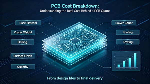
El presupuesto de una placa de circuito impreso puede variar sorprendentemente de un proveedor a otro, incluso cuando los archivos Gerber son idénticos.
El motivo es que el precio de las placas de circuito impreso no se basa en una única operación de fabricación.
El coste típico de producción de una placa de circuito impreso puede incluir:
- Materias primas
- Cobre
- Procesamiento de la capa interna
- Laminación
- Perforación
- Revestimiento
- Grabado
- Acabado superficial
- Máscara de soldadura y serigrafía
- Pruebas
- Herramientas y configuración
- Inspección de calidad
- Embalaje
Algunas especificaciones tienen un impacto directo en el consumo de material, mientras que otras aumentan el número o la complejidad de los procesos de fabricación.
Comprender estos componentes del coste facilita mucho la evaluación de un presupuesto antes de realizar un pedido.
Índice
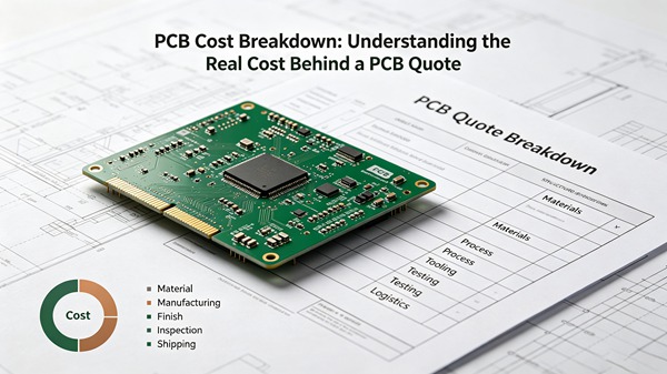
¿Qué se incluye en el coste de una placa de circuito impreso?
A grandes rasgos, el coste de los PCB se puede dividir en varias categorías:
| Categoría de costes | Factores habituales |
|---|---|
| Material | Laminado, cobre, preimpregnado |
| Fabricación | Impresión, grabado, laminado |
| Perforación | Número, tamaño y tipo de orificios |
| Revestimiento | Espesor del cobre, estructura de las vías |
| Acabado superficial | HASL, ENIG, OSP, etc. |
| Pruebas | Pruebas eléctricas, AOI, impedancia |
| Ingeniería | CAM, DFM, utillaje |
| Producción | Cantidad y eficiencia en la fabricación |
| Logística | Embalaje y envío |
La proporción exacta varía considerablemente en función de la estructura del PCB.
En una placa sencilla de dos capas, los costes de material y de configuración pueden ser los más importantes, mientras que en una placa HDI compleja los costes de procesamiento e ingeniería pueden ser mucho más elevados.
1. Coste del material de los circuitos impresos
El material es uno de los factores más evidentes que influyen en el precio de las placas de circuito impreso.
La estructura básica del material incluye:
- Lámina de cobre
- Núcleo
- Preimpregnado
- Resina
- Fibra de vidrio
En el caso de las placas estándar, el FR-4 es un material muy utilizado.
Las aplicaciones más exigentes pueden requerir:
- FR-4 de alta Tg
- Materiales de bajas pérdidas
- Materiales a base de PTFE
- Laminados de alta frecuencia
- Materiales para núcleos metálicos
La selección de materiales debe ajustarse a los requisitos eléctricos y ambientales de la aplicación.
Elegir un laminado más caro sin una razón técnica supone un aumento del coste sin que ello suponga necesariamente una mejora del producto final.
2. Coste del cobre
El cobre influye directamente en el coste de los materiales de una placa de circuito impreso.
Entre los pesos de cobre más habituales se encuentran:
- media onza
- 1 onza
- 2 oz
- 3 oz
- 4 oz o más
Un mayor peso de cobre implica una mayor cantidad de cobre y también puede requerir procesos de grabado y galvanoplastia más exigentes.
En el ámbito de la electrónica de potencia, puede ser necesario utilizar cobre de gran espesor para:
- Mayor capacidad de corriente
- Mejor disipación del calor
- Menor resistencia del conductor
Por lo tanto, el peso del cobre debe seleccionarse en función de los requisitos eléctricos, en lugar de limitarse a elegir la especificación más baja disponible.
3. Número de capas
El número de capas influye considerablemente en el coste de fabricación.
Una placa de circuito impreso multicapa puede requerir varios:
- Operaciones de obtención de imágenes de la capa interna
- Ciclos de laminación
- Operaciones de perforación
- Etapas del recubrimiento
- Pasos de la inspección
Por ejemplo, una placa de 8 capas no cuesta simplemente el doble que una de 4 capas.
La relación se ve afectada por:
- Apilamiento
- Composición del material
- Estructura de los orificios
- Cantidad de producción
- Complejidad del diseño
Véase también: Fabricación de placas de circuito impreso multicapa
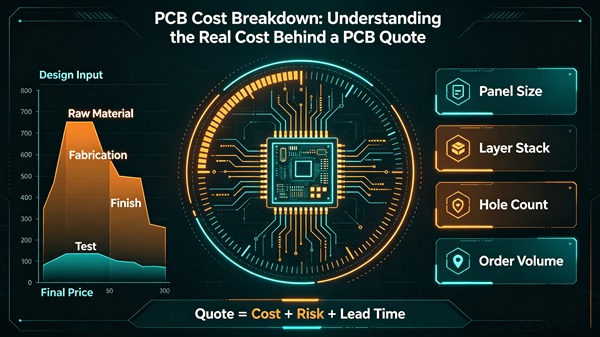
4. Tamaño de la placa y aprovechamiento del panel
Una placa de circuito impreso más grande consume más material.
Pero el aprovechamiento de los paneles es igual de importante.
Supongamos que un panel de producción tiene capacidad para:
- 10 placas en una sola disposición
pero una dimensión alternativa de la placa permite:
- 12 placas por panel
Es posible que el segundo diseño tenga un coste de material por placa de circuito impreso menor, aunque las dimensiones de cada placa sean prácticamente idénticas.
Por eso es importante tener en cuenta la panelización antes de fijar las dimensiones mecánicas definitivas.
Véase también: Directrices para la panelización de placas de circuito impreso
5. Coste de la perforación
El taladrado es otra parte fundamental de la fabricación de placas de circuito impreso.
Los orificios pasantes estándar son relativamente sencillos.
Los requisitos más complejos pueden aumentar los costes:
- Pequeños orificios mecánicos
- Un gran número de agujeros
- Vías ciegas
- Vías enterradas
- Microvías
- Taladrado inverso
La perforación con láser y las estructuras secuenciales requieren un procesamiento y un equipamiento adicionales.
Esta es una de las razones por las que una placa de circuito impreso HDI puede costar bastante más que una placa de circuito impreso multicapa convencional de tamaño similar.
6. Coste del recubrimiento
Tras el taladrado, se aplica un recubrimiento de cobre para establecer las conexiones eléctricas a lo largo de la placa.
Los requisitos de recubrimiento dependen de:
- Estructura de los orificios
- Espesor del cobre
- Relación de aspecto
- Requisitos de fiabilidad
Una mala calidad del recubrimiento puede provocar problemas de fiabilidad, como grietas en las vías y fallos en los tambores.
Véase también: Análisis de fallos en las vías de los circuitos impresos
Por este motivo, reducir los requisitos de recubrimiento únicamente con el fin de reducir los costes no suele ser una estrategia sensata.
7. Coste del acabado superficial
El acabado superficial influye tanto en el precio como en el rendimiento del montaje.
Entre las opciones más habituales se encuentran:
- HASL
- HASL sin plomo
- ENIG
- OSP
- Plata de inmersión
- Estanque de inmersión
El HASL suele resultar económico para aplicaciones convencionales.
Es posible que se opte por ENIG cuando el diseño requiera:
- Almohadillas planas
- Componentes de paso fino
- Montaje de BGA
- Mayor uniformidad de la superficie
El acabado adecuado depende del proceso de montaje y de la aplicación, más que del precio por sí solo.
8. Máscara de soldadura y serigrafía
La máscara de soldadura y la serigrafía suelen representar una parte menor del coste total de la placa de circuito impreso.
Sin embargo, los requisitos poco habituales pueden aumentar la complejidad del proceso.
Algunos ejemplos son:
- Colores especiales de máscara de soldadura
- Espacios reducidos entre las máscaras
- Eliminación selectiva de la máscara de soldadura
- Requisitos de marcado complejos
En la mayoría de los diseños estándar, estos costes son relativamente menores en comparación con los de los materiales, las capas, el taladrado y el acabado superficial.
9. Coste de las pruebas
Los requisitos de ensayo varían en función de la aplicación y la fase de producción.
Entre los métodos habituales de inspección y ensayo se incluyen:
AOI
La inspección óptica automatizada permite detectar defectos de fabricación como, por ejemplo:
- Pantalones cortos
- Abre
- Problemas con el grabado
- Problemas con el registro
Pruebas eléctricas
Las pruebas eléctricas verifican la continuidad y el aislamiento de los circuitos.
Pruebas de impedancia
Los diseños de alta velocidad pueden requerir una verificación de la impedancia controlada.
Inspección por rayos X
La inspección por rayos X resulta útil para examinar estructuras internas y determinados conjuntos complejos.
Cuanto más exigentes sean los requisitos de ensayo, mayor será el coste de producción asociado.
10. Costes de ingeniería y utillaje
No todos los costes de una placa de circuito impreso (PCB) se deben directamente a la placa física.
Antes de la producción, es posible que los equipos de ingeniería tengan que llevar a cabo:
- Análisis de Gerber
- Preparación de la CAM
- Revisión de DFM
- Generación de herramientas
- Panelización
- Verificación de la pila
Algunos proveedores cobran estos costes por separado, mientras que otros los incluyen en el presupuesto de las placas de circuito impreso.
Al comparar presupuestos, asegúrate de que estos elementos se comparen en las mismas condiciones.
11. Cantidad de producción
La cantidad influye considerablemente en el precio unitario.
En un pedido pequeño de prototipos, los costes fijos se reparten entre un número relativamente reducido de placas.
Por ejemplo:
Engineering + tooling + setup = fixed cost ↓ divided by quantity ↓ unit cost decreases
A medida que aumenta el volumen de producción, la eficiencia en la fabricación suele mejorar.
Sin embargo, encargar más placas de circuito impreso de las necesarias simplemente para conseguir un precio unitario más bajo puede aumentar el riesgo de exceso de existencias.
En el caso de los nuevos productos, suele ser más sensato validar primero el diseño y ampliar la producción posteriormente.
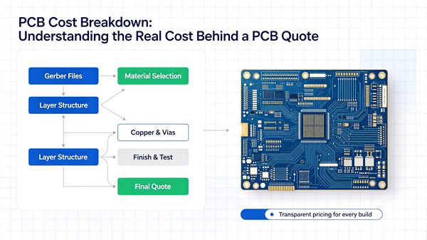
Por qué dos presupuestos de placas de circuito impreso pueden variar mucho
Imaginemos una placa de circuito impreso hipotética de cuatro capas.
El proveedor A ofrece un precio bajo.
El proveedor B ofrece un precio un 30 % más alto.
A primera vista, el proveedor A parece ser la mejor opción.
Sin embargo, la cotización puede basarse en supuestos distintos.
Por ejemplo:
| Artículo | Cita A | Cita B |
|---|---|---|
| Material | FR-4 estándar | FR-4 de alta Tg |
| Cobre | 1 onza | 1 onza |
| Acabado superficial | HASL | ENIG |
| Pruebas | Eléctrico | Eléctrica + AOI |
| Tolerancia | Estándar | Más ajustado |
| Embalaje | Estándar | Protección contra la humedad |
En realidad, los dos precios no se refieren a requisitos de fabricación idénticos.
Por eso La comparación de precios siempre debe comenzar con la comparación de las características técnicas..
Guía práctica: Cómo comparar correctamente dos presupuestos de placas de circuito impreso
Paso 1: Comparar el material
Comprueba:
- Tipo de laminado
- Tg
- Dk/Df, si procede
- Construcción con núcleo y prepreg
No te limites a comparar solo las palabras «FR-4».
Paso 2: Comparar la estructura de las capas y del cobre
Confirmar:
- Número de capas
- Peso del cobre
- Cobre interno
- Cobre exterior
Paso 3: Comparar los requisitos de los orificios
Comprueba:
- Ejercicio mínimo
- Número de orificios pasantes
- Vías ciegas
- Vías enterradas
- Microvías
- Taladrado inverso
Paso 4: Comparar el acabado de la superficie
Asegúrate de que ambos presupuestos especifiquen el mismo acabado.
El ENIG y el HASL no deben considerarse opciones de fijación de precios equivalentes.
Paso 5: Comparar pruebas
Pregunta si el precio presupuestado incluye:
- Prueba eléctrica
- AOI
- Prueba de impedancia
- Rayos X
- Pruebas de fiabilidad
Paso 6: Comparar la cantidad y el plazo de entrega
Un precio unitario bajo puede depender de un mayor volumen de producción o de un plazo de entrega más largo.
Paso 7: Comparar el coste final de entrega
Piénsalo:
Precio de la placa de circuito impreso + utillaje + pruebas + embalaje + envío
Esto permite realizar una comparación mucho más realista.
Cómo reducir el coste de los PCB sin mermar la fiabilidad
La reducción de costes debería centrarse en eliminar la complejidad innecesaria, en lugar de suprimir los controles de calidad necesarios.
Buenas oportunidades para reducir costes
- Optimizar el número de capas
- Utiliza materiales estándar cuando sea adecuado
- Mejorar el aprovechamiento de los paneles
- Evita las tolerancias innecesariamente ajustadas
- Reducir los procesos especiales innecesarios
- Elige un acabado adecuado
- Optimizar la cantidad de producción
Estrategias inadecuadas de reducción de costes
- Reducir el contenido de cobre por debajo de los requisitos eléctricos
- Uso de un laminado inadecuado
- Suprimir las pruebas necesarias
- Reducir el recubrimiento por debajo de los requisitos de fiabilidad
- Elegir un proceso que no pueda cumplir de forma sistemática con los requisitos de diseño
El segundo grupo puede rebajar el presupuesto inicial, pero aumentar el coste total más adelante.
Cuando una placa de circuito impreso más cara resulta, en realidad, más barata
Un precio más elevado de las placas de circuito impreso puede, en ocasiones, reducir el coste total del producto.
Por ejemplo, una placa de circuito impreso más resistente puede reducir:
- Defectos de montaje
- Fallos en el terreno
- Reelaboración
- Reclamaciones de garantía
- Paradas en la producción
Esto es especialmente importante en:
- Electrónica del automóvil
- Controles industriales
- Equipo médico
- Electrónica de potencia
- Productos de alta fiabilidad
Por lo tanto, los ingenieros deberían tener en cuenta coste total de propiedad, en lugar de centrarse únicamente en el precio unitario inicial de la placa de circuito impreso.
FAQ
R: El coste de una placa de circuito impreso suele incluir los materiales, la fabricación, el taladrado, el recubrimiento, el acabado superficial, las pruebas, la ingeniería y los gastos relacionados con la producción.
R: Las capas adicionales requieren más procesos de laminación, exposición, taladrado, recubrimiento e inspección.
R: Sí. Los costes fijos de ingeniería y puesta en marcha se reparten entre un mayor número de placas a medida que aumentan los volúmenes de producción.
R: Las especificaciones de los materiales, los acabados superficiales, los requisitos de ensayo, las tolerancias, las cantidades de producción y los plazos de entrega pueden influir en el presupuesto.
R: El enfoque más eficaz consiste en eliminar la complejidad innecesaria en la fabricación, manteniendo al mismo tiempo intactos los requisitos eléctricos, mecánicos y de fiabilidad.
Conclusión
Un presupuesto de una placa de circuito impreso (PCB) supone mucho más que el coste del laminado y del cobre.
El precio final depende de toda la cadena de fabricación:
Material → Layer Structure → Drilling → Plating → Surface Finish → Testing → Production Volume
A la hora de comparar presupuestos de placas de circuito impreso, los ingenieros deben asegurarse primero de que las especificaciones sean realmente equivalentes.
La mejor estrategia para reducir costes no consiste en elegir la opción de fabricación más barata, sino en diseñar y fabricar la placa de circuito impreso con solo la complejidad que la aplicación realmente requiere.
Este enfoque ofrece un mejor equilibrio entre el precio, la facilidad de fabricación, la fiabilidad y el coste del producto a largo plazo.
 ES
ES  EN
EN  PT
PT  AR
AR  DE
DE  FR
FR