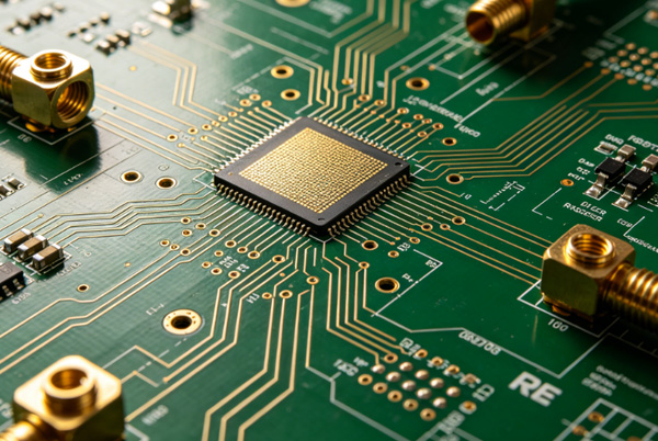
As processing speeds and component density continue to increase, many advanced electronic systems require more routing layers and better signal isolation than lower-layer-count boards can provide.
An 18 layer PCB offers additional signal layers, multiple reference planes, and improved power distribution, making it suitable for complex designs involving high pin-count devices and high-speed interfaces.
Typical applications include:
- AI servers
- Telecommunications equipment
- Aerospace electronics
- High-performance computing systems
- Medical imaging equipment
- Industrial control platforms
TOPFAST provides custom 18 layer PCB manufacturing for prototype and production requirements, with support for controlled impedance and advanced multilayer structures.
Table of Contents
Why Use an 18 Layer PCB?
Compared with 10- or 12-layer boards, an 18-layer structure offers greater routing flexibility and improved electrical performance.
Higher Routing Density
Additional layers simplify the routing of:
- Large BGA packages
- DDR memory interfaces
- PCIe buses
- High-speed differential pairs
This allows designers to reduce board size while maintaining signal quality.
Improved Signal Integrity
Multiple ground planes help:
- Reduce crosstalk
- Improve the return current paths
- Minimize reflections
Related Reading: PCB Stackup Design Guide
Better Power Distribution
Additional power and ground layers contribute to:
- Lower PDN impedance
- Reduced switching noise
- Improved voltage stability
Enhanced EMI Performance
More reference layers improve shielding and help reduce electromagnetic interference.
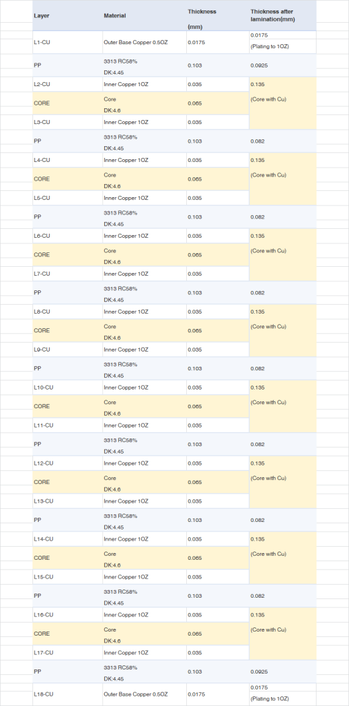
Typical 18 Layer PCB Stackup
A common stackup configuration is shown below:
L1   Signal
L2   Ground
L3   Signal
L4   Ground
L5   Signal
L6   Power
L7   Ground
L8   Signal
L9   Signal
L10  Ground
L11  Power
L12  Signal
L13  Ground
L14  Signal
L15  Ground
L16  Signal
L17  Ground
L18  Signal
This structure provides:
- Stable impedance control
- Effective signal isolation
- Balanced copper distribution
- Improved EMI performance
Depending on the application, stackups may also be optimized for HDI structures or high-frequency designs.
Related Reading: High Frequency PCB Material Selection
Standard Specifications
| Parameter | Capability |
|---|---|
| Layer Count | 18 Layers |
| Material | FR4, High Tg FR4, Rogers |
| Copper Weight | 0.5–6 oz |
| Board Thickness | 1.6–6.0 mm |
| Minimum Trace/Space | 3/3 mil |
| Minimum Drill Size | 0.15 mm |
| Surface Finish | ENIG, HASL, OSP, Immersion Silver |
| Controlled Impedance | Supported |
| IPC Standard | IPC Class 2 / IPC Class 3 |
Material Options
Standard FR4
Standard FR4 is suitable for many industrial and embedded applications where cost and manufacturability are priorities.
High Tg Materials
High Tg laminates are commonly used in applications that experience:
- High operating temperatures
- Lead-free assembly processes
- Long service life requirements
Rogers Materials
Rogers laminates are typically selected for:
- RF circuits
- Microwave systems
- High-speed communication equipment
Common Applications
AI Servers and High-Performance Computing
Large processors and memory architectures require:
- Dense routing
- Stable power distribution
- Excellent signal integrity
Telecommunications Equipment
Applications include:
- Core network switches
- Optical communication systems
- 5G infrastructure
These systems require low-loss transmission and reliable impedance control.
Aerospace Electronics
Aerospace systems place high demands on:
- Reliability
- Thermal stability
- Resistance to vibration
Medical Equipment
Medical imaging systems and monitoring equipment benefit from multilayer structures that provide low noise and stable signal transmission.
Manufacturing Challenges
Producing an 18 layer PCB requires tighter process control than conventional multilayer boards.
Layer Registration
Accurate alignment between inner layers is critical to maintain hole quality and signal continuity.
Lamination Control
Multiple lamination stages require precise control of:
- Temperature
- Pressure
- Resin flow
Improper processing may lead to internal defects or reliability issues.
Related Reading: PCB Manufacturing Process
Warpage Control
As board thickness increases, maintaining flatness becomes more difficult.
Balanced copper distribution and symmetrical stackups help minimize:
- Bow and twist
- Mechanical stress
- Assembly problems
Design Considerations
Stackup Planning
Stackup design affects:
- Signal integrity
- EMI performance
- Manufacturability
Early stackup planning helps avoid costly redesigns.
Related Reading: PCB Stackup Design Guide
Controlled Impedance
Many 18-layer boards support interfaces such as:
- PCIe
- Ethernet
- USB
- DDR memory buses
Impedance requirements should be considered before layout begins.
Via Reliability
Deep vias and thicker boards require attention to:
- Aspect ratio
- Copper plating thickness
- Hole wall quality
Related Reading: PCB Via Failure Analysis
18 Layer PCB vs 16 Layer PCB
| Feature | 16 Layer PCB | 18 Layer PCB |
|---|---|---|
| Routing Density | Very High | Extremely High |
| Signal Integrity | Excellent | Superior |
| Power Integrity | Excellent | Better |
| Manufacturing Complexity | Very High | Higher |
| Typical Applications | AI Servers, Telecom | HPC, Aerospace, Networking |
How to Order a Custom 18 Layer PCB
- Step 1
Provide:
. Gerber files
. Layer stackup requirements
. Impedance specifications - Step 2
Confirm:
. Material selection
. Copper thickness
. Surface finish - Step 3
Engineering review and DFM analysis.
- Step 4
Prototype verification.
- Step 5
Mass production.
FAQ
A: 18 layer PCBs are widely used in AI servers, telecommunications equipment, aerospace electronics, and high-performance computing systems.
A: Common finished thicknesses range from 1.6 mm to 6.0 mm, depending on layer structure and copper weight.
A: Yes. Controlled impedance structures are commonly used in high-speed digital and communication applications.
A: Standard FR4, High Tg FR4, and Rogers materials are the most common choices.
A: Higher layer counts require more lamination cycles, tighter tolerances, and additional process control, increasing manufacturing complexity and cost.
Conclusion
An 18 layer PCB provides the routing density and electrical performance required by today’s advanced electronic systems. Through optimized stackup design, material selection, and controlled manufacturing processes, these boards support demanding applications in AI computing, telecommunications, aerospace, and industrial electronics.
 EN
EN  PT
PT  AR
AR  DE
DE  FR
FR  ES
ES