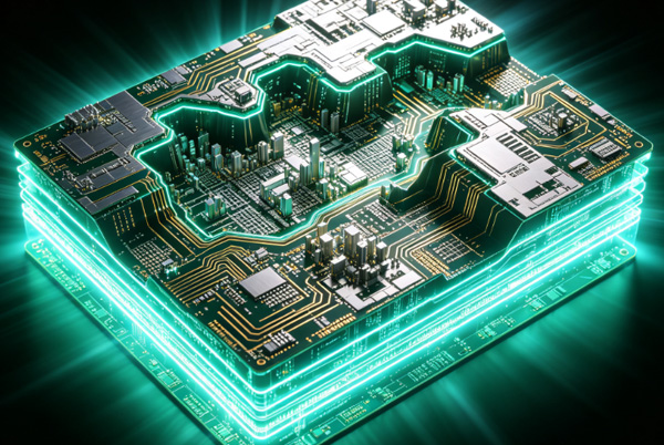
Modern electronic products continue to integrate more computing power, faster interfaces, and greater functionality into smaller footprints. As a result, many designs exceed the routing capacity of conventional multilayer boards.
A 20 layer PCB provides additional signal layers and reference planes that allow engineers to manage dense component layouts while maintaining signal integrity and power stability. It is commonly selected for systems that must support multiple high-speed interfaces, large processors, and demanding reliability requirements.
Typical applications include:
- AI computing platforms
- High-performance servers
- Telecommunications infrastructure
- Aerospace electronics
- Medical imaging systems
- Industrial automation equipment
TOPFAST manufactures custom 20 layer PCBs from prototype builds through volume production, supporting controlled impedance, advanced multilayer stackups, and engineering review before fabrication.
Table of Contents
Why Choose a 20 Layer PCB?
Compared with lower layer count boards, a 20-layer PCB offers greater flexibility for complex circuit design.
Increased Routing Capacity
Additional routing layers simplify the layout of:
- Large FPGA and CPU packages
- High-density BGA devices
- DDR memory channels
- PCIe and Ethernet interfaces
The extra routing space also reduces congestion around critical components, making signal routing more efficient.
Better Signal Integrity
Well-planned reference planes improve signal quality by:
- Reducing crosstalk
- Maintaining consistent return paths
- Minimizing signal reflections
These improvements become increasingly important as data rates continue to rise.
Related Reading: PCB Stackup Design Guide
Improved Power Distribution
Multiple power and ground planes help stabilize voltage delivery across the board, reducing power noise and supporting high-current devices.
Better EMC Performance
Proper layer arrangement helps contain electromagnetic radiation and reduces interference between adjacent signal layers.
Typical 20 Layer PCB Stackup
There is no universal stackup for every design, but a balanced arrangement similar to the example below is widely used.
L1   Signal
L2   Ground
L3   Signal
L4   Ground
L5   Signal
L6   Power
L7   Ground
L8   Signal
L9   Signal
L10  Ground
L11  Power
L12  Ground
L13  Signal
L14  Signal
L15  Ground
L16  Power
L17  Signal
L18  Ground
L19  Signal
L20  Signal
Actual stackups should always be developed according to:
- Signal speed
- Layer utilization
- Power requirements
- Manufacturing capability
For high-speed applications, stackup planning should be completed before PCB layout begins.
Related Reading: High Frequency PCB Material Selection
Typical Manufacturing Specifications
| Parameter | Capability |
|---|---|
| Layer Count | 20 Layers |
| Material | FR4, High Tg FR4, Rogers |
| Copper Weight | 0.5–6 oz |
| Board Thickness | 1.6–6.0 mm |
| Minimum Trace/Space | 3/3 mil |
| Minimum Drill Size | 0.15 mm |
| Surface Finish | ENIG, OSP, HASL, Immersion Silver |
| Controlled Impedance | Supported |
| IPC Standard | IPC Class 2 / IPC Class 3 |
Manufacturing capability may vary depending on board size, aspect ratio, copper thickness, and overall stackup complexity.
Material Selection
Standard FR4
For many industrial and computing applications, high-quality FR4 remains a practical choice when electrical loss requirements are moderate.
High Tg FR4
High Tg laminates are commonly selected where thermal reliability is important, such as automotive electronics, industrial equipment, and products that experience multiple lead-free soldering cycles.
Low-Loss Materials
For high-speed networking and RF applications, low-loss laminates help reduce insertion loss and improve signal integrity over long transmission paths.
Typical Applications
AI Servers
Modern AI hardware often combines multiple processors, high-speed memory, and complex power architectures on a single board. A 20-layer structure provides the routing resources needed to support these designs.
Telecommunications Equipment
Core network switches, optical transmission systems, and wireless infrastructure frequently require multilayer boards with controlled impedance and stable electrical performance.
Aerospace Electronics
Aerospace applications demand reliable multilayer PCBs capable of operating under vibration, temperature cycling, and other challenging environmental conditions.
Medical Imaging Equipment
Medical systems require stable signal transmission and low electrical noise, making multilayer stackups a common choice for imaging and diagnostic equipment.
Industrial Automation
Industrial control systems benefit from additional ground planes, improved EMC performance, and greater routing flexibility.
Manufacturing Considerations
Producing a 20-layer PCB involves significantly more process control than manufacturing conventional multilayer boards.
Inner Layer Registration
Precise alignment of each inner layer is essential to maintain reliable electrical connections throughout the board.
Lamination Process
Multiple lamination cycles require accurate control of temperature, pressure, and resin flow. Consistent process control helps reduce the risk of internal defects.
Related Reading: PCB Manufacturing Process
Hole Quality
As board thickness increases, plated through holes become more challenging to manufacture. Hole quality directly influences long-term reliability, particularly in applications exposed to thermal cycling.
Design Considerations
Plan the Stackup Early
Stackup planning should begin before routing. Decisions made at this stage influence signal integrity, manufacturability, and cost.
Reserve Continuous Reference Planes
High-speed signals perform more consistently when routed adjacent to uninterrupted ground planes.
Balance Copper Distribution
Balanced copper helps reduce mechanical stress during lamination and solder assembly, improving board flatness.
Work with Your PCB Manufacturer
High-layer-count boards often require adjustments to dielectric thickness, copper weight, and drill structures. Early communication with the fabrication team helps avoid unnecessary design revisions.
20 Layer PCB vs 16 Layer PCB
| Feature | 16 Layer PCB | 20 Layer PCB |
|---|---|---|
| Routing Density | Very High | Extremely High |
| Signal Integrity | Excellent | Outstanding |
| Power Distribution | Excellent | Superior |
| Design Complexity | High | Very High |
| Typical Applications | Telecom, AI Servers | HPC, Aerospace, Advanced Computing |
FAQ
A: 20 layer PCBs are commonly used in AI servers, telecommunications equipment, aerospace electronics, medical imaging systems, and other applications requiring dense routing and stable electrical performance.
A: No. The required layer count depends on routing complexity, component density, power distribution, and signal integrity requirements. Many products perform well with 8 to 16 layers.
A: Standard FR4, High Tg FR4, and low-loss laminates are commonly selected based on performance requirements.
A: Yes. Additional layers increase lamination steps, inspection requirements, and manufacturing complexity, resulting in higher production costs than lower layer count boards.
A: Yes. Controlled impedance is routinely implemented on 20-layer boards used for high-speed communication and computing applications.
Conclusion
A 20 layer PCB offers the routing density, electrical performance, and reliability required for today’s most demanding electronic systems. With proper stackup planning, suitable material selection, and close collaboration between designers and manufacturers, high-layer-count PCBs can deliver consistent performance in applications ranging from AI computing and telecommunications to aerospace and industrial automation.
 EN
EN  PT
PT  AR
AR  DE
DE  FR
FR  ES
ES