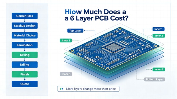
A 6 layer PCB is commonly used when a 4 layer design can no longer provide enough routing space, power distribution, or signal reference planes.
It is often found in:
- Industrial controllers
- Networking equipment
- Automotive electronics
- Embedded computing systems
- Communication equipment
- More complex consumer electronics
Adding two layers does increase manufacturing cost, but the difference is not determined by layer count alone.
A 6 layer PCB with standard FR-4, conventional through-holes, and moderate design rules can be relatively straightforward to manufacture.
A board with the same dimensions may become considerably more expensive when it also requires high-Tg material, heavy copper, controlled impedance, blind vias, or tight tolerances.
The useful question is therefore not simply “How much does a 6 layer PCB cost?”, but “What does this particular 6 layer construction require?”
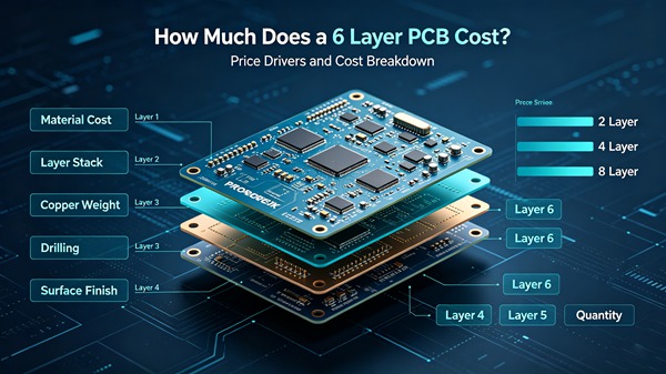
Table of Contents
Why Does a 6 Layer PCB Cost More Than a 4 Layer PCB?
The most obvious difference is the additional internal copper layers.
But manufacturing cost increases because the complete production structure becomes more involved.
A 6 layer PCB normally requires additional:
- Inner-layer imaging
- Prepreg and core materials
- Lamination
- Registration control
- Inspection
- Drilling and plating operations
The board therefore consumes more material and requires more processing than a conventional 4 layer PCB.
This does not mean the price is simply 50% higher.
Manufacturing costs contain both fixed and variable components, so the actual difference depends heavily on board size, quantity, materials, and fabrication requirements.
The Stackup Has a Major Influence on Cost
Not every 6 layer PCB uses the same construction.
A typical design might use:
- Layer 1: Signal
- Layer 2: Ground
- Layer 3: Signal
- Layer 4: Power
- Layer 5: Ground
- Layer 6: Signal
Another design may use a different arrangement depending on:
- High-speed interfaces
- Power requirements
- Impedance targets
- EMI considerations
- Component placement
The stackup determines the type and thickness of core and prepreg materials required.
It also affects impedance, signal return paths, and manufacturing tolerances.
When evaluating a 6 layer quotation, the stackup should be treated as part of the technical specification rather than just a purchasing detail. See PCB Stackup Design for the design considerations behind multilayer construction.
Board Size Still Matters
A larger 6 layer PCB consumes more laminate and copper.
However, panel utilization can make the relationship less obvious.
For example, changing the board outline by a few millimeters may allow an additional PCB to fit on the production panel.
That can reduce material waste and improve the unit economics of the order.
For production designs, it is therefore worth reviewing the board outline together with the manufacturing panel rather than optimizing the two separately.
Material Selection
Standard FR-4 is suitable for many 6 layer applications.
More demanding designs may require:
- High-Tg FR-4
- Low-loss materials
- High-frequency laminates
- Low-CTE materials
The material affects more than the initial quotation.
It also influences:
- Thermal stability
- Z-axis expansion
- Signal performance
- Lamination behavior
- Reliability
For a conventional industrial controller, standard FR-4 may be sufficient.
For a high-speed communication board, material selection becomes much more important.
Copper Weight and Power Requirements
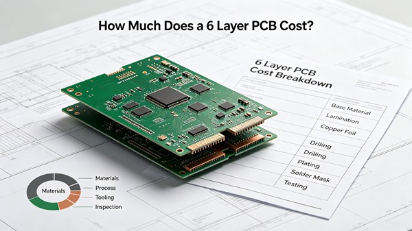
Many 6 layer PCBs use 1 oz copper, but this depends on the application.
Higher copper weight can be required for:
- High-current power paths
- Power conversion
- Thermal management
- Low-resistance conductors
The cost impact comes from both copper consumption and the additional processing needed for heavier copper.
A common mistake is to specify heavy copper on every layer when only certain power layers require it.
A more efficient design can use different copper weights where the manufacturing process allows it.
Via Structure
A conventional 6 layer PCB can often be manufactured using through-hole vias.
This keeps the fabrication relatively straightforward.
Cost can increase when the design requires:
- Blind vias
- Buried vias
- Microvias
- Backdrilling
- Very small mechanical holes
For example, a 6 layer board with standard through-holes is fundamentally different from a 6 layer HDI construction, even if the external dimensions are identical.
The latter requires additional fabrication stages and tighter process control.
This is why HDI PCB Manufacturing should be considered a separate cost category rather than simply another layer-count option.
Minimum Trace Width and Spacing
A 6 layer PCB gives designers more routing space, which can sometimes make it possible to use more conventional trace geometry.
This is an important point.
Adding layers does not always increase cost in every area.
A design that moves from 4 to 6 layers may actually become easier to manufacture if the additional routing space allows:
- Wider traces
- Larger clearances
- Fewer vias
- Less congested routing
So although the additional layers add cost, they may eliminate other expensive design features.
This is one reason why optimizing purely for the lowest layer count can produce the wrong result.
Controlled Impedance
For high-speed 6 layer boards, impedance requirements can influence the stackup and material selection.
The manufacturer may need to control:
- Dielectric thickness
- Trace width
- Copper thickness
- Reference-plane position
- Material Dk
More demanding impedance tolerances require tighter process control.
If the design has high-speed interfaces, impedance should therefore be considered during stackup development rather than added after the PCB has already been routed.
Surface Finish
Surface finish usually has less influence on total cost than layer count or material, but it still affects the quotation.
Common options include:
- HASL
- Lead-free HASL
- ENIG
- OSP
- Immersion silver
For a conventional through-hole or larger-pad SMT design, HASL may be sufficient.
For fine-pitch components or applications requiring a flatter surface, ENIG may be more appropriate.
The correct choice depends on the assembly requirements.
Quantity Changes the Unit Price
The unit price of a 6 layer prototype can look quite different from a production order.
Small quantities have to absorb fixed costs such as:
- CAM preparation
- Tooling
- Production setup
- Material preparation
With larger quantities, these costs are distributed across more boards.
However, a higher quantity is not automatically better.
For a new product, the design may still change after:
- Functional testing
- EMC testing
- Thermal testing
- Mechanical validation
Producing a large quantity before those stages are complete can create obsolete inventory.
Lead Time and Expedited Production
A standard 6 layer board requires more processing than a simple 2 layer PCB.
If a project requires an unusually short lead time, production scheduling can become more difficult.
Before choosing an expedited option, check:
- Material availability
- Required lamination schedule
- Special process requirements
- Testing requirements
A realistic standard lead time is often preferable to rushing a complex board through production.
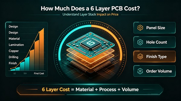
When Is Moving From 4 Layers to 6 Layers Worth the Cost?
This is one of the most important engineering decisions.
Adding two layers can make sense when a 4 layer design is becoming difficult to route.
For example, a 6 layer structure may provide:
- Dedicated ground planes
- Better power distribution
- More routing channels
- Better signal reference
- Reduced via congestion
It can also help reduce the need for extremely narrow traces.
In some cases, the extra PCB fabrication cost is offset by a simpler layout and fewer design compromises.
A Simple Example
Imagine a product initially designed as a 4 layer PCB.
During routing, the engineering team discovers that:
- Several high-speed interfaces compete for the same routing area
- Ground return paths are interrupted
- Power routing occupies valuable signal space
- Additional vias are required
One option is to keep four layers and make the routing increasingly complicated.
Another is to move to six layers.
The six-layer board costs more to fabricate, but may provide:
- Cleaner signal routing
- Better reference planes
- Fewer vias
- Easier EMC control
- Better long-term design stability
In this situation, the additional PCB cost may be justified.
How-To: Reduce the Cost of a 6 Layer PCB
Step 1: Start With the Electrical Requirements
Before reducing cost, identify which layers are actually required for:
- Signal routing
- Power
- Ground
- Impedance control
Do not remove a layer that is serving an important electrical purpose.
Step 2: Use a Practical Stackup
Avoid unnecessarily exotic material constructions.
If standard FR-4 provides adequate performance, it may be the more economical option.
Step 3: Keep Vias Simple
Use standard through-hole vias where the design permits.
Do not introduce HDI structures unless they solve a genuine routing or mechanical problem.
Step 4: Review Copper Requirements
Use heavier copper where current or thermal requirements justify it rather than applying the same heavy copper specification everywhere.
Step 5: Check Panel Utilization
Review the PCB outline before production.
A small mechanical adjustment may improve the number of boards per panel.
Step 6: Compare Complete Quotations
Compare:
- Material
- Stackup
- Copper weight
- Surface finish
- Quantity
- Testing
- Lead time
A cheaper quotation with different material or testing assumptions is not necessarily cheaper on an equivalent basis.
6 Layer PCB Cost Compared With Other Layer Counts
| PCB Type | Relative Complexity | Typical Reason for Use |
|---|---|---|
| 2 layer | Low | Simple electronics |
| 4 layer | Moderate | General multilayer designs |
| 6 layer | Moderate–high | More routing and better plane management |
| 8 layer | High | Dense/high-speed designs |
| 10+ layer | Very high | Complex computing, networking, industrial systems |
These are relative comparisons rather than fixed price multipliers.
A small 8 layer PCB may sometimes cost less than a large or unusually specified 6 layer board.
That is why actual quotations need to be based on the complete design.
FAQ
A: It is normally more expensive because of additional material and fabrication steps, but the actual difference depends on board size, quantity, material, copper weight, and via structure.
A: The additional layers can provide more routing space, dedicated power and ground planes, better signal reference, and fewer routing compromises.
A: Yes. Many 6 layer boards use standard FR-4 when their electrical and thermal requirements allow it.
A: No. Many 6 layer boards can be manufactured entirely with conventional through-hole vias. Blind or buried vias should be used when there is a specific design reason.
A: Start by reviewing the stackup, material, copper weight, via structure, board dimensions, and production quantity. Avoid special processes that do not provide a real engineering benefit.
Conclusion
A 6 layer PCB costs more than a basic 4 layer board because it requires additional materials and fabrication steps. But the additional cost can be worthwhile when the extra layers solve routing, power distribution, signal integrity, or EMC problems.
The best way to control cost is not to force every design into the fewest possible layers.
Instead, look for a balanced construction:
appropriate layer count + practical stackup + suitable material + simple via structure + efficient panelization
For a new 6 layer design, this evaluation should happen before the Gerber files are released. Early stackup and DFM review can preven
 EN
EN  PT
PT  AR
AR  DE
DE  FR
FR  ES
ES