Modern electronics manufacturing demands far more than simple board fabrication and component placement. As electronic designs transition toward high-density interconnects (HDI), fine-pitch array packages, and high-frequency signal processing, managing fragmentation across different vendors poses major production risks.
For hardware projects that utilize complex multilayer PCB stackups, dense BGA devices, or controlled-impedance routing, any disconnect between the PCB fabricator and the SMT assembly line can cause severe manufacturing bottlenecks, field failures, or unexpected lead-time delays.
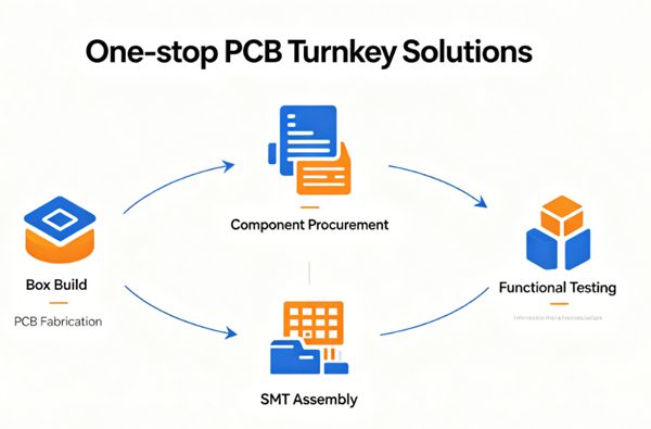
In traditional manufacturing, managing separate vendors for PCB fabrication, component procurement, and PCBA assembly often leads to communication gaps and finger-pointing when quality issues arise. PCB turnkey solutions eliminate this fragmentation. By unifying the entire production lifecycle—from engineering review and parts procurement to final SMT assembly and functional testing—Original Equipment Manufacturers (OEMs) can drastically reduce time-to-market while ensuring complete product traceability.
At Topfast, we leverage our integrated engineering and manufacturing systems to deliver scalable turnkey solutions for industrial control systems, automotive electronics, advanced IoT hardware, and medical communication equipment.
Table of Contents
What Are PCB Turnkey Solutions?
A PCB turnkey solution is an end-to-end electronics manufacturing model where a single contract manufacturer (CM) takes full responsibility for the entire production workflow. Instead of the client coordinating multiple procurement and manufacturing streams, the turnkey partner handles everything under one roof based on the client’s design files (Gerbers, BOM, and Centroid data).
Depending on your internal supply chain strategy and inventory commitments, turnkey services are typically divided into two models:
Full Turnkey vs. Partial Turnkey Manufacturing
Service Comparison: Choosing Your Production Model
| Manufacturing Phase | Full Turnkey Services | Partial (Consigned) Turnkey |
| PCB Fabrication | Managed entirely by Topfast | Managed entirely by Topfast |
| Component Procurement | 100% sourced via authorized distributors | Core ICs/MCUs supplied by client; passives/standard parts sourced by Topfast |
| Incoming Quality Control (IQC) | Full counterfeit verification & date code tracking | Verification of client-supplied parts + incoming inspection of sourced parts |
| Production Preparation | Unified DFM/DFA engineering review | Unified DFM/DFA engineering review |
| Best Suited For | Fast-turn prototyping, NPI, and highly scalable mass production | Proprietary IC silicon, existing inventory utilization, or restricted supply chains |
Full Turnkey Manufacturing
In a full turnkey project, the manufacturer manages the entire stack: raw material sourcing, PCB fabrication, Bill of Materials (BOM) procurement, SMT and through-hole (THT) assembly, firmware flashing, and rigid testing. This model is highly optimized for New Product Introduction (NPI) and agile hardware development, as any component footprint mismatches or stackup anomalies are caught and resolved internally before production scheduling begins.
Partial Turnkey Manufacturing
Partial turnkey (or consigned) manufacturing allows clients to maintain control over specific, high-value, or long-lead components (such as specialized custom MCUs, proprietary FPGAs, or legacy connectors) while outsourcing the procurement of standard passive components (resistors, capacitors, diodes) and PCB fabrication to the manufacturing partner. This model provides supply chain flexibility without sacrificing assembly efficiency.
Internal Link Optimization: To learn more about our specific assembly capabilities, explore our comprehensive guide on PCB Assembly Services and specialized SMT Assembly Services.

Cross-Disciplinary Engineering Review Before Fabrication
The foundation of a reliable turnkey assembly run happens long before the SMT line starts moving. Front-end engineering review is where manufacturing yield is won or lost. Our engineering team conducts rigorous pre-production analysis to bridge the gap between your CAD layout and actual shop-floor realities.
1. Gerber and PCB Fabrication Validation
Before sending the layout to fabrication, we run comprehensive checks on design parameters to ensure stable material processing:
- Trace and Space Integrity: Verifying copper spacing, minimum trace widths, and via aspect ratios to guarantee high plating reliability in multilayer structures.
- Stackup and Impedance Control: Reviewing core/prepreg thickness definitions and dielectric constants ($D_k$) to ensure critical high-speed signals match target impedance calculations.
- Drill and Annular Ring Tolerances: Checking for sufficient pad sizes around vias to prevent breakout defects during mechanical or laser drilling.
2. BOM Integrity & Component Lifecycle Scrubbing
Component procurement is one of the highest-risk phases in the electronics supply chain. Before our purchasing team issues any POs, your BOM undergoes a strict lifecycle analysis:
- Obsolescence and NRND Status: Identifying End-of-Life (EOL) or Not Recommended for New Design (NRND) components that could jeopardize long-term production.
- Footprint and Package Cross-Checks: Cross-referencing manufacturer part numbers (MPNs) against the Gerber layout footprints to eliminate package mismatches (e.g., trying to place a 0402 component onto a 0603 pad).
- Drop-in Alternatives: Prequalifying alternative components based on electrical parameters, thermal performance, and pin-compatibility to hedge against sudden supply allocation.
3. Rigid DFM & DFA Analysis
Design for Manufacturability (DFM) and Design for Assembly (DFA) ensure that your boards pass through our high-speed pick-and-place lines with maximum first-pass yield:
- Tombstoning Prevention: We optimize thermal relief and copper balance on passive pads to ensure uniform heat distribution, preventing uneven surface tension during reflow.
- Component Clearances: Verifying spacing around larger components, BGAs, and QFNs to allow adequate clearance for placement nozzles, automated inspection, and rework equipment.
- Fiducial Mark Optimization: Ensuring precise global and local fiducial placements on the panel layout to achieve exact optical alignment on our SMT lines.
Internal Link Optimization: Working with advanced layouts? Check out our technical breakdowns on Multilayer PCB Manufacturing and high-density HDI PCB solutions.
Mitigating Component Sourcing and Supply Chain Risks
Global electronics supply chains require proactive, engineering-driven procurement strategies. At Topfast, we combat common sourcing bottlenecks through a multi-tiered supply chain security protocol.
Eliminating Long Lead-Time Delays
Critical silicon like power management ICs (PMICs), microcontrollers, and wireless modules frequently suffer from erratic market lead times. Our supply chain team actively monitors component distribution networks, utilizing rolling production forecasts and secure buffer stocks of long-lead items to prevent assembly line stoppages.
Anti-Counterfeit Mitigation Pipeline
Counterfeit components threaten product reliability and intellectual property. We mitigate this risk through a strict incoming material inspection pipeline:
- Authorized Channels: We procure components exclusively through original component manufacturers (OCMs) or top-tier franchised global distributors (e.g., Arrow, DigiKey, Mouser, Avnet).
- Strict IQC Protocol: Incoming components undergo date code validation, manufacturer labeling verification, and physical packaging checks. For high-risk or legacy parts requested by clients, we utilize X-ray inspection and electrical characteristics testing to ensure 100% authenticity.
Internal Link Optimization: Need details on individual component tracking? See how we manage supply networks on our Electronic Components procurement page.
SMT Assembly Process Control & Thermal Profiling
High-yield SMT production requires a relentless focus on process variables, thermal physics, and real-time optical inspection.
Precision Solder Paste Printing & 3D SPI
Statistically, over 60% of SMT assembly defects originate from poor solder paste printing. We control this phase by:
- Custom-engineering laser-cut electro-polished stencils with optimized aperture aspect ratios.
- Deploying automated 3D Solder Paste Inspection (SPI) immediately post-print to measure paste volume, height, and alignment, instantly gating out any defects before component placement.
Ultra-Accurate Component Placement
Our production lines utilize high-speed automated SMT placement systems capable of mounting fine-pitch ICs, 0201 passives, and complex BGA/QFN packages with precise, repeatable component alignment. Real-time component verification systems ensure right-first-time feeding.
Scientific Reflow Thermal Profiling
To achieve robust, void-free solder joints across mixed-technology assemblies without damaging sensitive components, our engineers build dedicated thermal profiles for every unique board geometry. We tightly regulate:
- Preheat and Soak Zones: Actively monitoring the ramp rate to prevent thermal shock to ceramic capacitors and components.
- Time Above Liquidus (TAL) & Peak Temperature: Ensuring lead-free paste reaches full wetting flow (typically peaking around 240°C–260°C) while verifying that heavy ground planes and small passives reach thermal equilibrium simultaneously, preventing board warpage.
Automated Inspection Matrix (AOI & 3D X-Ray)
- Automated Optical Inspection (AOI): Post-reflow, high-resolution multi-angle camera systems inspect 100% of the panel run for component presence, polarity, shifting, and solder bridging.
- 3D X-Ray Inspection (AXI): For hidden solder architectures such as BGA ball grids, QFN pads, and LGA packages, we use non-destructive X-ray imaging to check for internal voiding, solder ball bridging, and head-in-pillow (HIP) defects.
Comprehensive Testing and Quality Assurance
A successful turnkey delivery means boards arrive fully functional, certified, and ready for deployment. We implement a rigorous testing matrix tailored to your system requirements.
- In-Circuit Testing (ICT) & Flying Probe: ICT utilizes dedicated bed-of-nails fixtures to check component values, open circuits, and short circuits rapidly on medium-to-high volume runs. For prototypes and agile NPI production, our automated Flying Probe Testing systems scan the board via movable test probes without requiring custom tooling fixtures.
- Functional Circuit Testing (FCT): We simulate your product’s actual operating environment. Our technicians utilize custom functional test jigs to cycle power, flash system firmware, verify communication protocols (e.g., CAN bus, I2C, SPI, Wi-Fi/Bluetooth), and calibrate analog signals to guarantee the assembly performs flawlessly in the field.
- Rigorous Traceability & MES Integration: Operating under strict quality management systems (such as ISO 9001 and IPC-A-610 Class 2/3 requirements), we track production lots through an integrated Manufacturing Execution System (MES). This provides full component-level and process-level traceability for every PCBA shipped.

How to Get Started with Topfast PCB Turnkey Solutions
How-to Guide: Requesting an Optimized Turnkey Quote
Follow these 4 straightforward steps to submit your engineering data for an optimized, fast-turn PCB turnkey quote:
- Step 1: Prepare Your ODB++ or Gerber Data
Export your complete layout files (RS-274X or ODB++ format), including all copper layers, solder mask and silkscreen layers, drill files, and a detailed mechanical fabrication drawing outlining board dimensions and tolerances.
- Approved Alternate Parts (Optional): Specifying acceptable substitutes prevents sourcing stalls.
Ensure your BOM sheet is exported in Excel (.xls/.xlsx) or CSV format and contains the following mandatory data columns:
Manufacturer Part Number (MPN): Exact vendor part code.
Designator: Component references matching your layout (e.g., C1, R10, U3).
Manufacturer Name: (e.g., Texas Instruments, Murata).
Component Description: Package style and values (e.g., 10uF, 0603, 16V).
Quantity per board.
Approved Alternate Parts (Optional): Specifying acceptable substitutes prevents sourcing stalls. - Step 3: Provide Pick-and-Place (Centroid) Coordinates
Include the component placement XY data file (frequently called the Centroid, Pick-and-Place, or XY file) containing reference designators, X/Y locations, board layer, and rotation angles to automate SMT program setup.
- Step 4: Define Testing and Assembly Parameters
Specify your assembly requirements: Full Turnkey or Partial Turnkey, required build volume, IPC classification (Class 2 or Class 3), RoHS compliance needs, and any specialized functional testing guidelines or enclosure assembly (box build) drawings. Submit these directly to our RFQ engineering portal for a rapid review.
FAQ
A: To generate an accurate turnkey quote, you must provide your PCB Gerber files (RS-274X or ODB++), a complete Bill of Materials (BOM) containing Manufacturer Part Numbers (MPN) and quantities, a Centroid/Pick-and-Place file for SMT line programming, and explicit assembly specifications (such as copper weight, surface finish, and volume).
A: At Topfast, we mitigate counterfeit risk by procuring components exclusively through franchised global distributors and original component manufacturers (OCMs). All incoming components undergo rigorous Incoming Quality Control (IQC) validation, including label tracking, date-code checks, and visual package verification before line release.
A: In a full turnkey assembly, the manufacturer completely manages the raw board fabrication, 100% component sourcing, SMT/THT assembly, and final testing. In Partial Turnkey assembly, the client ships critical or proprietary components (consigned inventory) to our facility, while we source the remaining standard passives, fabricate the PCBs, and perform assembly.
A: Yes. Turnkey manufacturing is highly beneficial for New Product Introduction (NPI) and engineering prototypes. It eliminates the logistical nightmare of engineers sourcing small part quantities from multiple vendors and shipping them manually, allowing engineering teams to focus purely on design verification.
A: Because the solder connections on Ball Grid Array (BGA) and Quad Flat No-Lead (QFN) packages are physically hidden beneath the component body, standard visual or AOI inspection cannot verify their integrity. We utilize automated 3D X-Ray Inspection (AXI) to view through the packages, evaluating solder ball alignment, wetting quality, and internal void percentages.
A: PCB warpage during assembly is primarily caused by structural thermal stresses. This occurs if there is an asymmetrical layer stackup layout, uneven copper density distribution across opposing layers, or an incorrect thermal reflow profile where thermal ramp-up and cooling rates are not strictly regulated to match the substrate’s Coefficient of Thermal Expansion (CTE).
A: Yes. Our turnkey manufacturing pipelines operate under a strict quality management matrix. Our assembly processes comply fully with IPC-A-610 Class 2 and Class 3 (for high-reliability medical/automotive/industrial systems) standards, backed by certified ISO 9001 production facilities.
Conclusion
As modern PCB designs push the boundaries of signal speeds, component densities, and thermal constraints, reliable hardware deployment depends entirely on unifying fabrication, component sourcing, and SMT processing under a singular, engineering-led pipeline.
PCB turnkey solutions fundamentally streamline your electronic product development lifecycle. By consolidating vendor management into a cohesive ecosystem, OEMs successfully eliminate sourcing friction, accelerate time-to-market, and guarantee end-to-end component traceability. For projects requiring multilayer architectures, advanced surface mount precision, or rigorous IPC validation, an engineering-driven turnkey partner like Topfast provides the visibility and process consistency needed to transition smoothly from prototype to volume production.