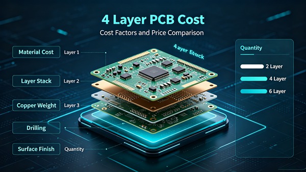
A 4 layer PCB is one of the most common multilayer configurations used in electronic products.
It provides more routing space than a 2 layer board while remaining considerably simpler and less expensive than high-layer-count or HDI constructions.
But there is no single price for a 4 layer PCB.
Two boards with the same dimensions can have noticeably different prices because of differences in:
- PCB material
- Copper weight
- Board thickness
- Surface finish
- Hole size and quantity
- Trace and spacing requirements
- Quantity
- Testing
- Production lead time
For this reason, a useful 4 layer PCB cost estimate should start with the complete manufacturing specification rather than board dimensions alone.
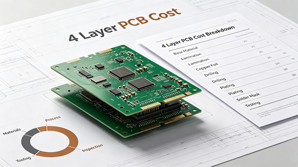
Table of Contents
What Is a Typical 4 Layer PCB?
A conventional 4 layer board commonly consists of:
- Top signal layer
- Ground or power layer
- Ground or power layer
- Bottom signal layer
The actual stackup depends on the application.
For a relatively simple controller board, two internal layers may primarily provide power and ground planes. For a high-speed design, the stackup may be arranged around controlled impedance and well-defined signal return paths.
This is one reason why 4 layer PCB price should not be judged only by layer count.
The layer count tells you the basic structure, but not the manufacturing difficulty.
For more information on the broader fabrication sequence, see PCB Manufacturing Process.
What Determines the Cost of a 4 Layer PCB?
Board Size
Board dimensions are one of the easiest cost factors to understand.
A larger board requires more laminate material and normally occupies more space on the production panel.
However, the relationship is not always linear.
A board measuring 100 × 100 mm does not necessarily cost twice as much as a 50 × 100 mm board because manufacturers also consider how efficiently the boards can be arranged on a panel.
For this reason, changing the outline slightly can sometimes improve material utilization.
Material Selection
Standard FR-4 is commonly used for 4 layer PCBs.
Depending on the application, designers may specify:
- Standard Tg FR-4
- High-Tg FR-4
- Low-loss materials
- High-frequency laminates
A standard digital controller may not need an expensive RF laminate.
On the other hand, a board operating at high frequency or in a demanding thermal environment may require a material with more stable electrical or thermal characteristics.
Using the cheapest laminate is therefore not necessarily the best way to reduce PCB cost.
Copper Weight
1 oz copper is common for many 4 layer designs.
Higher copper weights can increase material and processing costs.
For example, a power board may require 2 oz copper or more because of current and thermal requirements.
The important point is to distinguish between required copper weight and unnecessarily heavy copper.
If the traces and power distribution do not require additional copper, specifying it simply because it appears more robust can increase cost without providing a meaningful benefit.
PCB Thickness
Common board thicknesses are generally easier to manufacture than unusual constructions.
Cost can increase when a project requires:
- Non-standard thickness
- Tight thickness tolerance
- Unusual dielectric construction
- Special mechanical requirements
If the enclosure allows it, using a conventional board thickness can make procurement simpler.
Surface Finish
Surface finish can make a noticeable difference to the quotation.
Common options include:
- HASL
- Lead-free HASL
- ENIG
- OSP
- Immersion silver
HASL is often suitable for conventional applications.
ENIG is more expensive but may be appropriate where a flatter surface is needed, particularly with fine-pitch components.
The choice should therefore be based on assembly requirements rather than simply selecting the lowest-priced finish.
Drill Size and Hole Count
A standard 4 layer PCB with conventional through-holes is relatively straightforward to manufacture.
The cost can increase when the design contains:
- Very small mechanical holes
- Large numbers of holes
- Tight annular rings
- Blind vias
- Buried vias
- Microvias
A 4 layer board using standard through-hole vias can therefore have a very different price from a 4 layer board incorporating HDI structures.
A useful comparison is the more complex fabrication required for HDI PCB manufacturing.
Trace Width and Spacing
Most standard 4 layer boards do not require extremely fine traces.
When the design approaches a manufacturer’s process limits, fabrication becomes more demanding.
For example, unnecessarily tight:
- Line width
- Line spacing
- Annular ring
- Solder mask clearance
can increase manufacturing difficulty.
If the electrical design allows a more conventional geometry, relaxing these requirements can sometimes reduce cost and improve production yield at the same time.
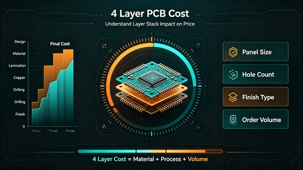
Surface Finish and Assembly Requirements
PCB cost should also be considered together with the assembly process.
A board designed for fine-pitch BGA or other dense SMT components may need a surface finish and pad structure that support reliable assembly.
For such designs, choosing a cheaper PCB finish can create additional assembly problems later.
This is particularly important for boards where PCB fabrication and SMT assembly are closely linked.
Quantity Has a Major Effect on Unit Price
The difference between prototype and production pricing can be significant.
A small order still requires:
- CAM preparation
- Tooling
- Production setup
- Material preparation
- Testing
These costs are distributed across a relatively small number of boards.
As quantity increases, the fixed portion of the cost is spread over more units.
For example, the unit price for:
10 boards
will normally be much higher than the unit price for:
1,000 boards
But ordering thousands of boards only to obtain a lower unit price is not always sensible for a new product.
If the design is still changing, excess inventory can become more expensive than the higher prototype price.
Lead Time Can Affect the Quotation
A standard production schedule is usually easier to plan than an urgent build.
Expedited production may involve:
- Priority production slots
- Additional process coordination
- Material availability constraints
- Overtime or scheduling adjustments
When comparing quotations, it is therefore useful to compare price and lead time together.
A quotation that is slightly cheaper but arrives two weeks later may not actually be the better choice for a product launch.
How-To: Estimate the Cost of a 4 Layer PCB Before Requesting a Quote
Step 1: Define the Basic Board Specification
Prepare:
- Board length and width
- Layer count
- Board thickness
- Copper weight
- Quantity
These provide the basic framework for the quotation.
Step 2: Identify Special Requirements
Check whether the design requires:
- Controlled impedance
- Small holes
- Blind or buried vias
- Special materials
- Heavy copper
- Unusual tolerances
If none of these are required, the board may be relatively straightforward to manufacture.
Step 3: Select the Surface Finish
Choose the finish according to the assembly requirements.
Do not specify ENIG simply because it is commonly used if HASL or another finish is adequate for the product.
Step 4: Review the Stackup
A 4 layer board does not have to use the same stackup for every application.
For high-speed designs, the relationship between signal layers, reference planes, and dielectric thickness becomes important.
This is also where your PCB Stackup Design content can naturally support the topic.
Step 5: Compare Equivalent Quotations
When comparing prices, make sure all quotations use the same:
- Material
- Copper weight
- Surface finish
- Board thickness
- Quantity
- Tolerances
- Testing requirements
Otherwise, the lowest number may simply represent a different specification.
What Makes a 4 Layer PCB More Expensive?
A relatively economical 4 layer PCB might use:
- Standard FR-4
- Standard thickness
- 1 oz copper
- Standard through-holes
- Conventional trace width and spacing
- Standard surface finish
- Moderate production volume
Cost increases when the same board requires several special processes.
For example:
| Specification | Cost Impact |
|---|---|
| Standard FR-4 | Lower |
| High-Tg material | Higher |
| 1 oz copper | Standard |
| 2 oz+ copper | Higher |
| Standard through-holes | Lower |
| Microvias | Higher |
| HASL | Usually lower |
| ENIG | Usually higher |
| Standard thickness | Lower |
| Special thickness | Higher |
| Larger quantity | Lower unit cost |
| Small prototype quantity | Higher unit cost |
The important observation is that not every expensive specification is unnecessary.
If a product needs high-Tg material or controlled impedance, those requirements are part of the engineering solution rather than optional costs.
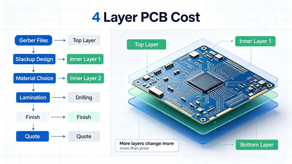
When Should You Choose 4 Layers Instead of 2?
Cost should not be the only consideration.
A 4 layer PCB may be justified when a 2 layer design creates problems with:
- Routing density
- Ground continuity
- Power distribution
- EMI
- Signal integrity
- Board size
Adding two layers can sometimes make the overall product cheaper because it simplifies routing and reduces board area.
For example, a compact controller may be easier to manufacture as a 4 layer PCB than as a much larger 2 layer board with complicated routing.
This is why the lowest PCB layer count does not always produce the lowest overall product cost.
4 Layer PCB Cost vs Higher Layer Counts
A 4 layer board is generally a practical starting point for many moderately complex products.
As layer count increases, additional lamination and fabrication steps become necessary.
| PCB Structure | Typical Complexity |
|---|---|
| 2 layer | Low |
| 4 layer | Moderate |
| 6 layer | Higher |
| 8 layer | Higher |
| 10+ layer | Complex |
For products that require more routing capacity, a higher layer count may be justified.
However, moving from 4 layers to 6 or 8 layers should be based on actual routing, power, mechanical, or signal-integrity requirements rather than simply following a standard design pattern.
How to Reduce 4 Layer PCB Cost
There are several practical ways to reduce cost without compromising reliability.
Use Standard Materials
If standard FR-4 meets the application’s requirements, there may be little benefit in using a specialized laminate.
Avoid Unnecessary Fine-Line Features
Do not design at the edge of manufacturing capability unless the layout genuinely requires it.
Optimize the Board Outline
A small change in dimensions can sometimes improve panel utilization.
Keep the Via Structure Simple
Standard through-hole vias are generally less expensive than blind, buried, or microvia structures.
Choose an Appropriate Surface Finish
Select the finish according to the assembly process rather than defaulting to the most expensive option.
FAQ
A: There is no universal price because board dimensions, material, copper weight, surface finish, quantity, and manufacturing requirements can vary significantly. A meaningful quotation requires the actual PCB specification and production quantity.
A: Compared with a 2 layer PCB, a 4 layer board requires additional lamination and fabrication processes. However, it remains one of the more common and cost-effective multilayer configurations.
A: Standard FR-4 is generally more economical than specialized high-frequency or high-performance laminates when it meets the application’s requirements.
A: ENIG generally costs more than HASL because it involves additional surface-finishing processes. Whether the difference matters depends on order quantity and the application.
A: Sometimes, but not always. A 2 layer design may require a larger board, more complicated routing, or additional compromises in power and signal integrity. The complete design should be evaluated before reducing layer count.
Conclusion
The cost of a 4 layer PCB is determined by much more than the number of layers.
The major factors are:
- Board size
- Material
- Copper weight
- Thickness
- Hole structure
- Surface finish
- Design tolerances
- Quantity
- Testing
- Lead time
For most projects, the best approach is to start with the simplest construction that satisfies the electrical, mechanical, thermal, and reliability requirements.
A well-designed 4 layer PCB does not need to use expensive materials or complicated fabrication processes unless the application actually requires them. Careful stackup planning, reasonable design rules, and appropriate material selection can often reduce cost while making the board easier to manufacture.
For a PCB quotation, the most useful comparison is therefore not simply “Which supplier is cheaper?”, but “Are both quotations based on the same engineering requirements?”
 EN
EN  PT
PT  AR
AR  DE
DE  FR
FR  ES
ES