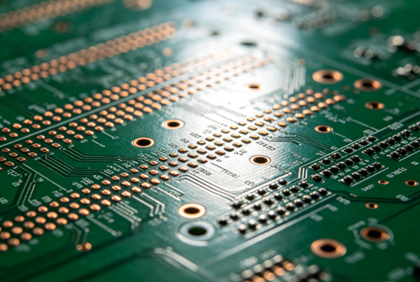
As electronic products continue to integrate more functionality and higher data rates, PCB structures become increasingly complex. A 14 layer PCB provides additional routing resources, enhanced power distribution, and better signal isolation than 8-layer or 12-layer boards.
These boards are commonly found in:
- AI servers
- High-performance computing systems
- Telecommunications equipment
- Networking switches
- Aerospace electronics
- Industrial control systems
- Medical imaging equipment
Compared with lower layer count boards, 14-layer PCBs offer:
- Higher routing density
- Superior signal integrity
- Better EMI suppression
- Improved power integrity
- Increased design flexibility
TOPFAST provides prototype and volume production for complex multilayer PCB projects with engineering support and DFM review.
Table of Contents
Why Use a 14 Layer PCB?
Support for High-Density Routing
Large BGAs, DDR memory buses, and high-speed interfaces require additional routing channels.
A 14-layer structure helps designers:
- Reduce PCB size
- Improve component placement flexibility
- Support complex processor architectures
Superior Signal Integrity
Multiple ground reference planes help:
- Minimize crosstalk
- Reduce reflections
- Improve return current paths
- Stabilize differential pairs
Related Reading: PCB Stackup Design Guide
Better Power Integrity
Additional power and ground layers improve:
- Voltage stability
- Noise suppression
- Switching performance
This becomes increasingly important for:
- CPUs
- FPGAs
- AI accelerators
Reduced Electromagnetic Interference
Dedicated shielding layers help reduce:
- EMI emissions
- Radiation noise
- Signal coupling
Related Reading: PCB Impedance Control Explained
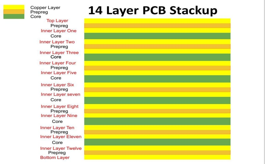
Typical 14 Layer PCB Stackup
A common stackup arrangement is:
L1   Signal
L2   Ground
L3   Signal
L4   Ground
L5   Signal
L6   Power
L7   Ground
L8   Ground
L9   Power
L10  Signal
L11  Ground
L12  Signal
L13  Ground
L14  Signal
Advantages:
- Excellent impedance control
- Improved EMI performance
- Strong signal isolation
- Balanced mechanical structure
Alternative stackups can be optimized for:
- High-speed digital systems
- RF applications
- HDI boards
- High-current power electronics
Related Reading: High Frequency PCB Material Selection
Standard 14 Layer PCB Specifications
| Parameter | Capability |
|---|---|
| Layer Count | 14 Layers |
| Material | FR4, High Tg FR4, Rogers |
| Copper Weight | 0.5–4 oz |
| Board Thickness | 1.2–4.5 mm |
| Minimum Trace/Space | 3/3 mil |
| Minimum Drill Size | 0.15 mm |
| Surface Finish | ENIG, HASL, OSP, Immersion Silver |
| Controlled Impedance | Supported |
| IPC Standard | IPC Class 2 / IPC Class 3 |
Material Options
Standard FR4
Suitable for:
- Industrial electronics
- Embedded systems
- Networking products
High Tg FR4
Recommended for:
- Automotive electronics
- Lead-free assembly
- High-temperature environments
Advantages include:
- Improved thermal stability
- Reduced delamination risk
- Better long-term reliability
Related Reading: PCB Delamination Causes and Prevention
Rogers Materials
Commonly used in:
- RF communication
- Radar systems
- Microwave circuits
Typical materials include:
- RO4350B
- RO4003C
- RO3003
Related Reading: High Frequency PCB Material Selection
Applications of 14 Layer PCBs
AI Servers and Data Centers
Modern AI systems require:
- High-speed interconnects
- Dense BGA packages
- Multiple power domains
14-layer boards provide sufficient routing resources and electrical performance.
Telecommunications Equipment
Applications include:
- 5G infrastructure
- Optical transmission systems
- Core network equipment
These systems require:
- Controlled impedance
- Low insertion loss
- Excellent EMI performance
Aerospace Electronics
Aerospace applications demand:
- High reliability
- Resistance to vibration
- Thermal stability
Medical Imaging Systems
Medical equipment requires:
- Stable signal transmission
- Low noise
- Long-term reliability
Industrial Automation
Industrial controllers benefit from:
- Improved power integrity
- Enhanced EMC performance
- Higher reliability
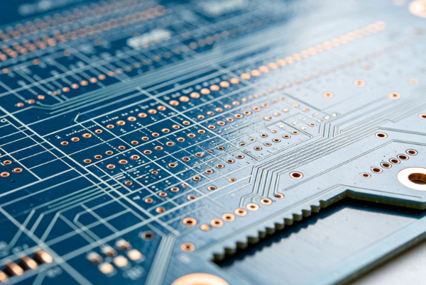
Manufacturing Challenges of 14 Layer PCBs
Compared with 8-layer or 10-layer boards, 14-layer structures present additional manufacturing complexity.
Layer Registration Accuracy
Inner layer alignment becomes increasingly critical.
Poor registration may cause:
- Via failures
- Impedance variations
- Signal discontinuities
Related Reading: PCB Via Failure Analysis
Lamination Process Control
Multiple lamination cycles require precise control of:
- Temperature
- Pressure
- Resin flow
Improper control can lead to:
- Delamination
- Internal voids
- Reliability issues
Related Reading: PCB Delamination Causes and Prevention
Warpage Control
Thicker multilayer structures are more susceptible to:
- Bow and twist
- Thermal deformation
- Mechanical stress
Related Reading: PCB Warpage and Reflow Deformation
Design Considerations
PCB Stackup Design
Stackup planning affects:
- Signal integrity
- Power integrity
- Manufacturability
Internal Link: PCB Stackup Design Guide
Controlled Impedance
Typical impedance values include:
| Interface | Typical Impedance |
|---|---|
| Ethernet | 100 Ω Differential |
| PCIe | 85 Ω Differential |
| USB | 90 Ω Differential |
| DDR | 40–60 Ω Single Ended |
Related Reading: PCB Impedance Control Explained
Via Reliability
High layer count boards place more stress on plated holes.
Design considerations include:
- Aspect ratio
- Copper thickness
- Hole wall quality
Related Reading: PCB Via Failure Analysis
Material Selection
Material choice should consider:
- Frequency requirements
- Thermal performance
- Reliability targets
Related Reading: High Frequency PCB Material Selection
14 Layer PCB vs 12 Layer PCB
| Feature | 12 Layer PCB | 14 Layer PCB |
|---|---|---|
| Routing Density | Very High | Higher |
| Signal Integrity | Excellent | Superior |
| Power Integrity | Excellent | Better |
| EMI Performance | Excellent | Outstanding |
| Manufacturing Complexity | High | Higher |
| Typical Applications | Networking, Telecom | AI Servers, Aerospace |
Related Reading: 12 Layer PCB Manufacturing
How to Order a Custom 14 Layer PCB
- Step 1
Submit:
. Gerber files
. Stackup requirements
. Impedance specifications - Step 2
Select:
. Material type
. Copper thickness
. Surface finish - Step 3
Engineering review and DFM analysis.
- Step 4
Prototype verification.
- Step 5
Mass production.
Frequently Asked Questions
A: 14 layer PCBs are widely used in AI servers, telecommunications equipment, aerospace systems, and industrial automation.
A: Yes. Fourteen-layer boards provide excellent signal integrity and controlled impedance performance.
A: Standard FR4, High Tg FR4, and Rogers laminates are commonly used.
A: Additional layers increase manufacturing complexity, lamination cycles, and process requirements.
A: Yes. Many 14-layer boards incorporate HDI technologies, blind vias, and buried vias.
Related Reading: Multilayer PCB Manufacturing
Conclusion
A 14 layer PCB delivers the routing density, electrical performance, and reliability required by advanced electronic systems.
Through optimized stackup design, controlled impedance, proper material selection, and robust manufacturing processes, 14-layer boards enable the development of AI servers, telecommunications infrastructure, aerospace systems, and other demanding applications.
 EN
EN  PT
PT  AR
AR  DE
DE  FR
FR  ES
ES