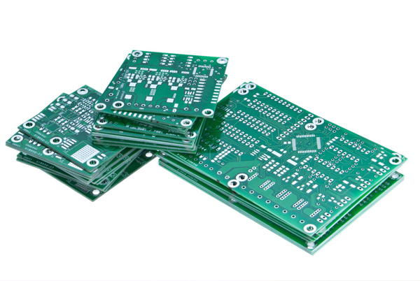
Four-layer PCB circuit boards have become the core components of communication equipment, medical instruments, industrial control systems, and high-end consumer electronics due to their excellent signal integrity, anti-interference capability, and high-density wiring characteristics. As a professional PCB manufacturer, we strictly control every detail of the four-layer board manufacturing process to ensure the performance and reliability of the final product.
Table of Contents
Detailed Explanation of 4-Layer PCB Manufacturing Process
1. Precision Stack-up Design
The 4-layer PCB adopts the classic “signal layer-ground layer-power layer-signal layer” structural design. This layered approach not only optimizes signal transmission paths but also significantly improves electromagnetic compatibility. Our engineers use professional simulation software for impedance matching calculations and signal integrity analysis to ensure high-frequency signal transmission quality.
During the stack-up design phase, we comprehensively consider the following factors:
- Precise control of dielectric layer thickness and dielectric constant
- Reasonable selection of copper foil thickness (typically 1oz for outer layers, 0.5oz for inner layers)
- Symmetrical structure design to reduce warpage risk
- Application planning of blind/buried via technology
2. High-Precision Inner Layer Production
Inner layer production is a critical link in 4-layer board quality. We employ industry-leading laser direct imaging (LDI) technology, achieving ultra-fine line width/spacing of ≤ 3 mil (0.075mm). Compared with traditional exposure technology, LDI offers the following advantages:
- No need for photomasks, reducing pattern transfer errors
- Higher resolution, suitable for HDI board production
- Shorter process time, improving production efficiency
The etching process uses acidic etching technology. By precisely controlling the temperature, concentration, and spray pressure of the etching solution, we ensure that c-side etching is controlled within 10%, achieving uniform line width accuracy.
3. Lamination Process
Lamination is the key process of combining each circuit board layer into a whole through prepreg. Our lamination process features include:
- Use of high-TG materials (such as FR-4 TG170) to ensure high-temperature reliability
- Vacuum lamination technology to eliminate bubble and delamination risks
- Precise temperature control (180±5℃) and pressure curves
- Strict control of the cooling process to reduce internal stress
After lamination, we conduct ultrasonic scanning to ensure no delamination or bubbles, with interlayer bonding force meeting IPC standards.
4. Drilling and Hole Metallization
Hole processing in 4-layer boards combines mechanical drilling and laser drilling technologies:
- Mechanical drilling: Suitable for ≥0.1mm through-holes and some blind vias
- Laser drilling: Used for <0.1mm microvias, with positioning accuracy of ±25μm
Hole metallization employs advanced chemical copper deposition processes, ensuring quality through the following steps:
- Desmear treatment: Remove resin residue from drilling
- Plasma treatment: Increase the hole wall roughness to enhance the bonding force
- Chemical copper deposition: Form uniform conductive layer (0.3-0.5μm)
- Panel plating: Thicken hole copper to 20-25μm
5. Outer Layer Pattern Transfer and Plating
Outer layer circuit production uses the pattern plating process:
- Dry film lamination: Apply photosensitive dry film on the copper surface
- Exposure and development: Form circuit pattern through LDI technology
- Pattern plating: Electroplate to thicken lines and hole copper
- Etching: Remove excess copper foil to form a final circuit
We use vertical continuous plating (VCP) lines, which offer better uniformity compared to traditional horizontal plating, with hole copper thickness variation controlled within ±5μm.
6. Surface Treatment: Ensuring Solderability Reliability
According to customer application requirements, we provide various surface treatment processes:
- ENIG: 1-2μm nickel layer + 0.05-0.1μm gold layer, suitable for high-reliability products
- HASL: Low cost, suitable for general applications
- OSP: Organic solderability preservative, suitable for short storage cycle products
- Immersion silver: Preferred solution for high-frequency applications
Each process is strictly controlled. For example, in the ENIG process, we control nickel layer phosphorus content at 7-9% to ensure solder joint strength and corrosion resistance.
7. Solder Mask and Legend Printing: Protection and Identification
The solder mask layer provides not only insulation protection but also affects product appearance. Our solder mask process features:
- Use of high-resolution LDI solder mask imaging, minimum opening 0.1mm
- Solder mask thickness 15-25μm, ensured through five pre-baking steps
- 100% solder mask coverage inspection to prevent exposed copper defects
Legend printing uses white or black ink to clearly mark component positions and board information, with positioning accuracy of ±0.1mm.
8. Routing and Final Inspection: Last Line of Quality Defense
Routing processing includes:
- CNC milling: Accuracy ±0.05mm
- V-CUT: Depth controlled at 1/3 of outer layer copper thickness
- Chamfering: Smooth edge treatment
Final inspection implements strict quality control:
- Visual inspection: 100% manual inspection + AOI automatic detection
- Electrical testing: Flying probe or test fixture, 100% coverage
- Impedance testing: ±10% tolerance for critical signal networks
- Reliability testing: Sampling for thermal stress, damp heat aging, etc.

Common Issues in 4-Layer PCB Production and Solutions
Issue 1: Interlayer Delamination in 4-Layer Boards
Root Cause Analysis:
- Improper lamination parameters (temperature/pressure/time)
- Material moisture absorption causes steam generation during lamination
- Poor inner layer copper surface treatment, insufficient bonding force
Solutions:
- Strictly control pre-lamination material baking conditions (typically 120℃×4 hours)
- Optimize the amination temperature profile to ensure complete resin flow
- Use black oxide or plasma treatment to increase the copper surface roughness
- Select PP sheets with high resin content to improve filling capability
Issue 2: How to Improve Failing Impedance Control?
Root Cause Analysis:
- Dielectric layer thickness variation
- Line width deviation exceeding allowable range
- Unstable material dielectric constant
Solutions:
- Adopt high-precision lamination control technology, thickness tolerance of ±5%
- Use LDI with an automatic line width compensation system
- Select low-DK-tolerance materials (e.g., FR408HR, DK tolerance ±0.2)
- Increase impedance test sample size for real-time feedback adjustment
Issue 3: Rough Hole Walls in 4-Layer Board Drilling
Root Cause Analysis:
- Drill bit wear or improper parameters
- Mismatch between the board resin system and drilling parameters
- Unsuitable entry/backup board selection
Solutions:
- Establish a drill bit life management system, and replace worn bits promptly
- Optimize drilling parameters (speed/feed rate) for different materials
- Use a dedicated aluminum entry board + phenolic backup board combination
- For high-TG materials, adopt the step drilling process
Core Advantages of a Professional PCB Manufacturer
Topfast, as a PCB manufacturer with 17 years of professional experience, possesses the following core advantages in 4-layer board production:
1. Advanced Production Equipment
- German LPKF laser drill (accuracy ±15μm)
- Japanese Mitsubishi LDI exposure machine (minimum line width 2 mil)
- Fully automatic VCP plating line (hole copper uniformity >85%)
- High-precision impedance test system (up to 40GHz)
2. Strict Quality System
- ISO9001, IATF16949 certified
- IPC-A-600G Class 3 standard implementation
- 18 quality control points at key processes
- SPC statistical process control implementation
3. Rapid Response Capability
- Sample lead time 5-7 days (industry average 10-12 days)
- 99.2% on-time delivery rate for mass production
- 24/7 online technical support
- Emergency order green channel
4. Extensive Product Experience
- Monthly capacity 100,000 square meters
- Over 50 million 4-layer boards produced cumulatively
- Mature special processes for high-frequency boards, heavy copper boards, blind/buried via boards, etc.
- Established stable cooperation with multiple Fortune 500 companies
Conclusion
The production of four-layer PCB boards is a systematic project that combines material science, precision processing, and quality control. From the stacked layer design to the final inspection, each link needs the support of specialized knowledge and rich experience. Choosing a professional PCB manufacturer not only ensures product quality but also provides significant advantages in the product development cycle and cost control.
Welcome to contact our engineers for free process consultation and quotation service, let us use our professional ability to protect your electronic products.