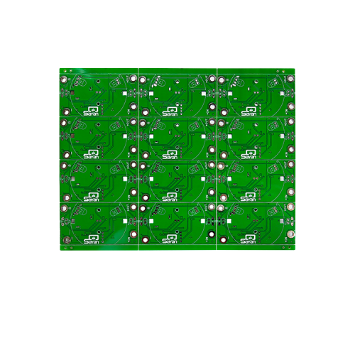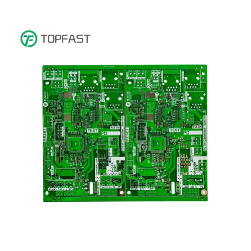
HDI PCB Manufacturing Services
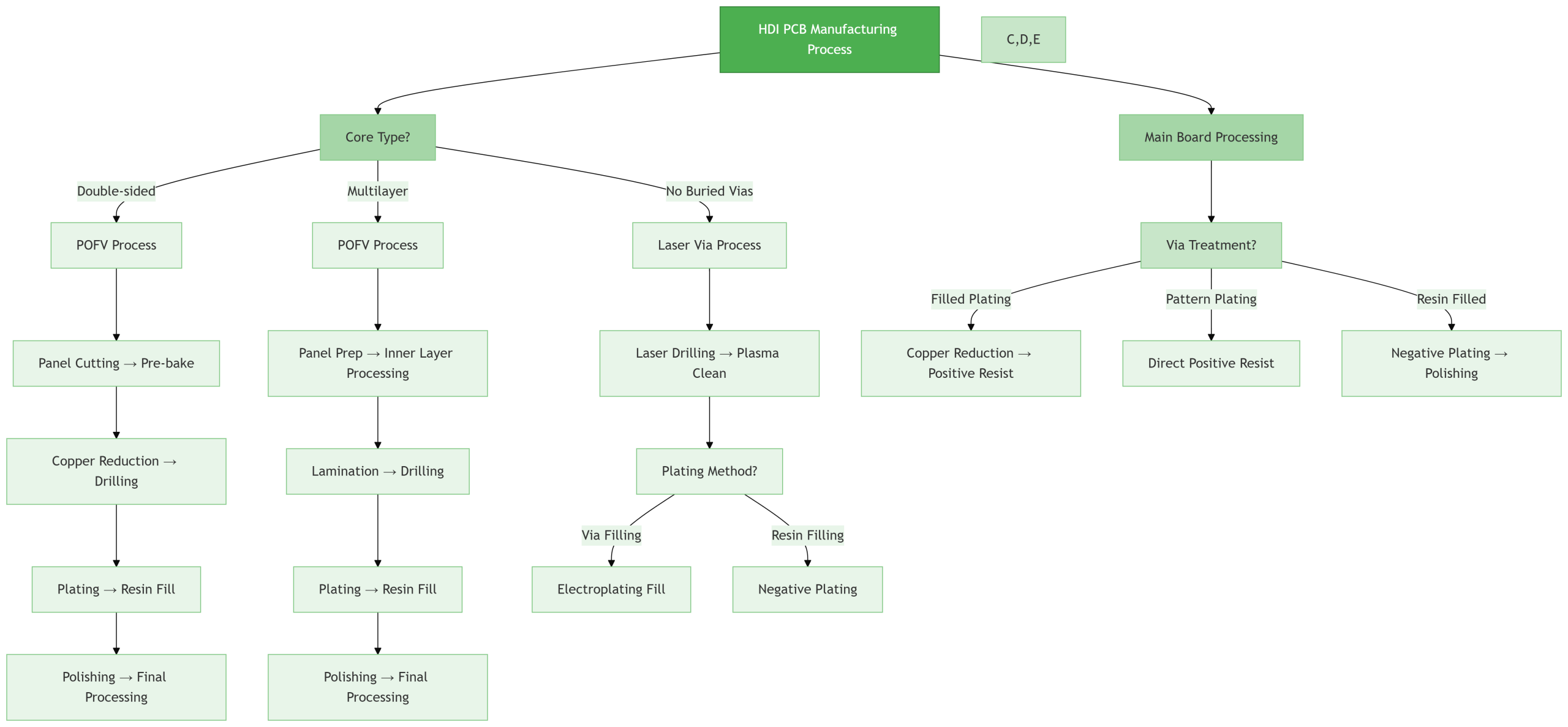
Topfast specializes in manufacturing high-density interconnect (HDI) PCBs with precision-engineered solutions, including blind vias, buried vias, microvias, and sequential lamination.
Leveraging cutting-edge production processes, we deliver superior performance, exceptional reliability, and compact designs tailored to meet the most demanding electronic applications.
Ultra-high density wiring
Utilizes laser microvia and blind/buried via technology
Advanced manufacturing processes
High-precision laser drilling, sequential lamination, ultra-thin dielectric materials
High reliability and stability
Strict quality control, high TG materials (Tg ≥ 170°C)
Fast delivery & cost optimization
Rapid prototyping for small to medium batches, cost reduction through large-scale production