Get a Quote
OUR BLOG
Focus on the latest articles that cover topics ranging from the latest technologies to best practices and industry news for PCB.
Mar 18, 2026
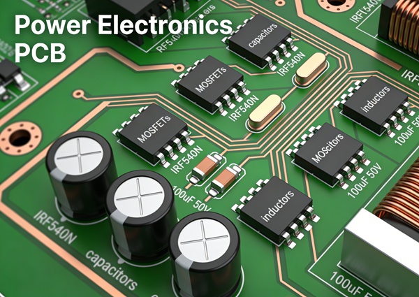
This article explores key design strategies for EV power electronics PCBs, including copper thickness selection, thermal management techniques, high-voltage spacing considerations, and stack-up optimization. It also discusses how PCB structure influences assembly reliability, particularly in high-power components and multilayer boards.
Mar 14, 2026
Mar 12, 2026
Detailed analysis of the key process points for PCB Via-in-Pad technology, comparing the differences between resin-filled vias and electroplated vias, providing a comprehensive guide from design to manufacturing, including parameter recommendations and quality control methods.
07
Nov
With the evolution of environmental regulations and market demands, halogen-free PCBs have become the mainstream choice in electronic design. This article outlines the international standards for halogen-free PCBs, highlights their significant advantages over traditional halogen-containing PCBs in thermal stability, electrical performance, and environmental safety, and provides key selection criteria for halogen-free laminates along with practical solutions for addressing design challenges.
06
The Core Knowledge System of Printed Circuit Boards (PCBs) provides comprehensive coverage from fundamental concepts to advanced technologies. Content includes detailed classifications of PCBs by substrate and structure, interpretation of key technical indicators such as board Tg values and Dk/Df parameters, step-by-step analysis of multilayer board manufacturing processes, and in-depth comparative analysis of various surface treatment techniques. This resource empowers informed decisions in PCB selection, design, and quality control.
30
Oct
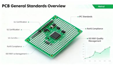
The universal standard system for printed circuit boards (PCBs) encompasses design specifications (e.g., IPC-6010), material standards (e.g., IPC-4101), soldering processes (e.g., J-STD-001), inspection methods (e.g., IPC-TM-650), and environmental requirements (e.g., IPC-1752). Ensuring PCB reliability and compliance under high-density, high-frequency, and harsh environmental conditions.
27
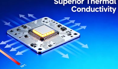
Aluminum-based PCBs (aluminum printed circuit boards) are specialized printed circuit boards utilizing aluminum alloy as the substrate material. Their three-layer structural design delivers exceptional thermal conductivity and electrical performance. Compared to traditional FR-4 PCBs, aluminum-based PCBs offer superior heat dissipation capabilities, high mechanical strength, and excellent dimensional stability.
24
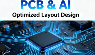
PCB: The Core Carrier and Performance Cornerstone of AI Hardware 1.1 Foundational Support Role Printed Circuit Boards (PCBs), serving as the “skeletal neural network” of electronic systems, play a key interconnection function within AI hardware architectures. In AI servers, edge computing devices, and intelligent terminals, high-performance PCBs are responsible for connecting GPU/TPU clusters, high-bandwidth memory […]
23
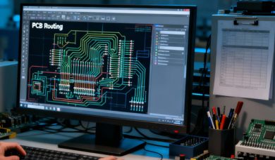
The 3W principle is a key design guideline for minimizing crosstalk in PCB routing, requiring that the center-to-center spacing between adjacent signal traces be no less than three times the trace width. Understanding the underlying physics, applicable scenarios, effectiveness evaluation, and practical considerations when applying this principle empowers engineers to significantly enhance signal integrity in high-speed circuit design.
22
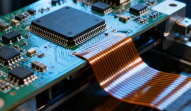
Understand the technical characteristics, application scenarios, and selection considerations for flexible PCBs and rigid-flex boards. By comparing differences with rigid PCBs and incorporating real-world application cases, this guide provides engineers with comprehensive decision-making references. It covers specific application solutions and design recommendations across multiple fields, ranging from consumer electronics to aerospace.
21
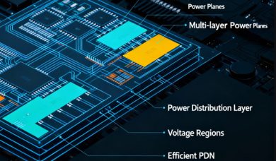
Analyzing the core elements of four-layer PCB design, including stackup selection, via parasitic parameter control, high-speed routing strategies, and power partitioning techniques, along with a design verification checklist to help engineers achieve high-reliability and signal-integrity circuit board designs.
18
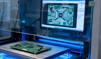
PCB characteristic inspection is a critical step in ensuring circuit boards meet design specifications and quality standards. This comprehensive checklist, covering electrical characteristic inspections and physical characteristic inspections, provides PCB design engineers with a complete quality control reference system.
17
A Comprehensive Guide to Letter Symbols for Electronic Components, including symbols, functions, and applications for capacitors, resistors, transistors, and other components.
16
Advanced PCB Layout Techniques From high-speed signal routing to impedance control, from power integrity optimization to thermal management strategies. Content covers key topics including differential pair routing, stackup design, decoupling capacitor placement, grounding techniques, and mixed-signal processing, helping engineers achieve optimal performance in high-frequency, high-speed circuit design.
15
Load More
Layers 1 Layers 2 Layers 4 Layers 6 Layers 8 Layers 10 Layers 12 Layers 14 Layers
Dimensions (mm)
Quantity 5 10 15 20 25 30 35 40 50 75 100 100+
Thickness 0.4mm 0.6mm 0.8mm 1.0mm 1.2mm 1.6mm 2.0mm 2.4mm
Quantity
Number of Unique Parts
SMT Pads
Thru-Holes