Table of Contents
What is Microvia Technology?
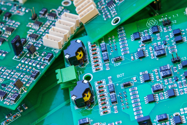
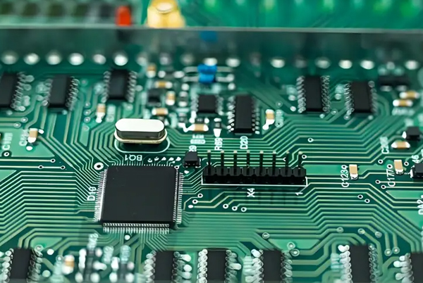
Microvia technology is a core process in modern high-density interconnect (HDI) printed circuit board manufacturing. It involves creating tiny conductive holes—typically less than 150 microns (0.15mm) in diameter—using laser drilling or other advanced methods. Compared to traditional mechanical drilling, microvia technology enables smaller apertures (as small as 0.05mm), higher positional accuracy (±0.01mm), and finer wiring density. This makes it possible to achieve high-density interconnections in complex PCB designs with 18 or more layers.
Microvia technology is mainly categorized into three types:
- Blind vias (from outer to inner layers, but not through the entire board)
- Buried vias (entirely between inner layers)
- Through vias (penetrating all layers)
In 18-layer PCBs, these microvia types are often combined to optimize routing solutions and signal integrity.
Core Advantages of Microvia Technology
- Significantly Improved Space Utilization – Microvias reduce aperture sizes to 1/4 or less of traditional drills, freeing up more routing space.
- Enhanced Signal Transmission Performance – Shorter interconnect paths minimize signal attenuation and delay, especially critical for high-frequency applications.
- Greater Flexibility in Layer Connections – Supports any-layer HDI (Any Layer HDI), increasing design freedom.
- Enables Product Miniaturization – Critical for thin and lightweight modern electronics (e.g., smartphones, wearables).
- Better Thermal Management – Microvia arrays can act as thermal channels, improving heat dissipation in multilayer PCBs.
Key Considerations for Microvia Design in 18-Layer PCBs
Achieving high-quality microvia interconnects in 18-layer PCB designs requires careful engineering:
1. Precision Control and Layer-to-Layer Alignment
- Problem: As layer count increases, cumulative alignment errors can cause microvia misregistration.
- Solution: Use high-precision laser drilling equipment (±5μm repeatability), real-time X-ray inspection for calibration, and incorporate process compensation in design.
2. Via Wall Quality and Plating Uniformity
- Problem: High aspect-ratio microvias may suffer from uneven plating or rough via walls.
- Solution: Optimize laser parameters (pulse width, energy), apply step-plating processes, and use additives to improve plating fluidity.
3. Thermal Stress and Reliability
- Problem: CTE (Coefficient of Thermal Expansion) mismatch in multilayer structures can lead to microvia cracking during thermal cycling.
- Solution: Select materials with matched CTE, use filled-via plating, and optimize hot air solder leveling (HASL) parameters.
Common Microvia Design Challenges and Solutions
Issue 1: Microvia Positional Errors Affecting Interconnect Reliability
Solution:
- Use optical positioning systems (OPS) combined with laser direct imaging (LDI).
- Follow a 1:1 via-to-pad ratio rule in design.
- Implement statistical process control (SPC) to monitor drilling accuracy.
Issue 2: Difficulty in Plating High Aspect-Ratio Microvias
Solution:
- Apply pulse-reverse plating for better deep-hole uniformity.
- Use specialized high-dispersion plating solutions.
- Implement vacuum-assisted plating to ensure full chemical penetration.
Issue 3: Microvia Deformation After Multiple Laminations
Solution:
- Optimize lamination cycles (step-wise temperature and pressure ramping).
- Choose low-resin-flow, high-Tg prepreg materials.
- Account for material shrinkage in design with proper compensation.
Industry Applications and Future Trends
Microvia technology plays a critical role in advanced applications:
- 5G Communications – Interconnects for millimeter-wave antenna arrays.
- High-Performance Computing (HPC) – 3D integration in multi-chip modules (MCMs).
- Automotive Electronics – High-reliability interconnects for ADAS systems.
- Medical Electronics – Ultra-dense interconnects in implantable microdevices.
As IC substrates and system-in-package (SiP) technologies evolve, microvia technology is advancing toward:
- Smaller sizes (≤50μm)
- Higher aspect ratios (>15:1)
- Tighter spacing (≤100μm pitch)
Emerging hybrid laser-plasma etching techniques may push these limits further.
Conclusion
Microvia design in 18-layer PCBs represents the pinnacle of modern interconnect technology, enabling macro-level performance breakthroughs through micro-scale precision engineering. Mastering microvia technology requires balancing design innovation with manufacturability—leveraging its high-density advantages while ensuring process feasibility and long-term reliability. With continuous advancements in materials and fabrication techniques, microvia technology will play an even more central role in next-generation electronics, driving progress toward higher performance, smaller form factors, and lower power consumption.
Read the latest articles
- The Ultimate Guide to HDI PCB Stack-up Design: From Basic Structures to Advanced Optimization Strategies
- Detailed Explanation of PCB V-Cut Panelization Technology
- PCB Assembly Design Guide
- How Flying Probe and Adapter Testing Are Reshaping PCB Quality Control Standards
- Mastering PCB Signal Integrity