Get a Quote
OUR BLOG
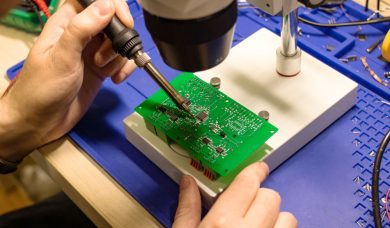
PCB design is a core aspect of electronic engineering, involving the conversion of circuit schematics into actual production-ready printed circuit board layouts, requiring comprehensive consideration of component layout, signal integrity, heat dissipation and electromagnetic compatibility.
29
Mar
Altium Designer is a powerful all-round PCB design tool, covering the schematic design to PCB layout of the full range of processes and other functions, to meet the needs of a variety of projects from simple to complex.
20
n the manufacture of electronic products, multi-layer PCB (printed circuit board) design and production is an indispensable key link, patchwork design (Panelization) is a PCB manufacturing process commonly used in a technology
18
Layers 1 Layers 2 Layers 4 Layers 6 Layers 8 Layers 10 Layers 12 Layers 14 Layers
Dimensions (mm)
Quantity 5 10 15 20 25 30 35 40 50 75 100 100+
Thickness 0.4mm 0.6mm 0.8mm 1.0mm 1.2mm 1.6mm 2.0mm 2.4mm
Quantity
Number of Unique Parts
SMT Pads
Thru-Holes