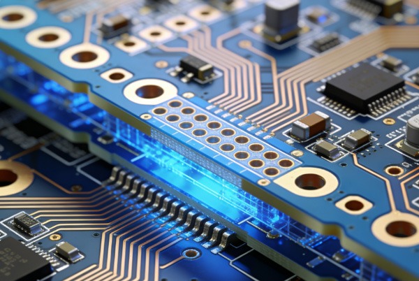
As electronic products rapidly develop towards miniaturization and high performance, traditional PCB technology can no longer meet the increasing demands for wiring density and signal integrity. HDI (High-Density Interconnect) PCB has become a core technology for implementing complex electronic system designs through microvia technology, multilayer stacking, and advanced materials. Whether facing the fan-out challenge of 0.4mm pitch BGA chips or the integrity requirements of high-speed signal transmission, a well-planned HDI stack-up design is key to success.
Table of Contents
Detailed Analysis of HDI Stack-up Structure Types
1.1 First-Order HDI (1+N+1 Structure)
- Structural Characteristics: The most basic HDI type, consisting of two outer layers (laser-drilled layers) and an N-layer core in between.
- Typical Applications: Medium-density consumer electronics, IoT devices, industrial controllers.
- Manufacturing Advantages: Completed in a single lamination cycle, mature process, and high cost-effectiveness.
- Design Example: 1+4+1 six-layer board, suitable for most applications with BGA pitch ≥0.5mm.
1.2 Second-Order HDI (2+N+2 Structure)
- Structure Classification:
- Staggered Via Design: Microvias on different layers are horizontally offset; a simple process, with high reliability.
- Stacked Via Design: Microvias are vertically stacked, saving space but requiring stringent manufacturing processes.
- Typical Applications: Smartphone motherboards, high-end routers, and medical imaging equipment.
- Technical Points: Requires two lamination cycles, supports finer line width/spacing (down to 3.0mil/3.0mil).
1.3 High-Order HDI and Any-Layer Interconnect
- Third-Order and Above Structures: Suitable for ultra-high-density scenarios such as AI chips and 5G RF modules.
- Any-Layer Interconnect (Anylayer): Allows direct connection between any adjacent layers, maximizing wiring freedom.
- Technical Challenges: Require multiple laminations, precise layer-to-layer alignment (within ±10μm), and advanced plating processes.
- Cost Considerations: Process complexity and cost increase exponentially with the number of sequential laminations.
Core Design Principles and Optimization Strategies
2.1 Design Specifications for Blind and Buried Vias
- Size Control: The aspect ratio of blind vias should be controlled at ≤1:1 to ensure plating quality and reliability.
- Spacing Requirements:
- Edge-to-edge spacing for blind vias of different nets: ≥9.5mil (0.24mm)
- Edge-to-edge spacing for blind vias of the same net: ≥5mil (0.13mm)
- Via-to-trace distance: Inner layer ≥6mil, outer layer ≥5-6mil
- Via-to-board-edge distance: ≥14mil (0.35mm)
- Process Selection:
- Stacked via designs must use electroplated via filling to ensure surface planarity.
- Resin plugging + electroplated capping is recommended for mechanically buried vias to prevent resin flow and voids.
2.2 Interlayer Structure and Signal Integrity Optimization
- Layer Stacking Strategy: Signal layers alternate with reference layers (GND/PWR).
- Recommended structure: Top signal – Layer 2 ground – Layer 3 power – Layer 4 signal.
- Advantages: Provides clear signal return paths, reduces crosstalk, and EMI radiation.
- Impedance Control:
- Precisely calculate microstrip and stripline dimensions, considering variations in material Dk values.
- High-speed differential signals require strict length matching, equal spacing, and parallel routing.
- Power Integrity:
- Avoid creating “islands” when splitting power planes to ensure uniform current distribution.
- Place decoupling capacitors close to ICs to reduce power noise.
2.3 Scientific Basis for Material Selection
- General Applications: FR-4 series meets most needs with good cost-effectiveness.
- High-Speed Scenarios: Low-loss materials (e.g., Rogers RO4835, Shengyi S1000-2M).
- Stable Dk values, low tanδ, suitable for applications above 5GHz.
- Excellent Anti-Conductive Anodic Filament (Anti-CAF) performance.
- Thermal Management Needs:
- Use metal-core substrates or heavy copper designs in high-power device areas.
- Optimize thermal conduction paths with thermal via arrays.
- Manufacturability Considerations: Avoid using more than three different types of prepreg to reduce thickness variation risks.
Key Points of Design for Manufacturability (DFM)
3.1 Lamination Process Optimization
- Minimizing Lamination Cycles: Reduce lamination cycles by optimizing buried via locations.
- Example: Changing buried vias from layers 3-6 to layers 2-7 can eliminate one lamination cycle.
- Lamination Strategy: Sequential lamination is preferable to single-step lamination for reducing bubbles and voids.
- Symmetrical Design: Even layer counts and symmetrical material distribution to reduce warpage risk.
3.2 Manufacturing Constraints and Design Adaptation
- Laser Drilling Capability: Minimum hole size 0.1mm (standard), 0.075mm (limit).
- Line Width/Spacing Limits: 3.0mil/3.0mil, meeting high-density routing requirements.
- Alignment Accuracy: Layer-to-layer alignment must be controlled within ±10μm to ensure microvia connection reliability.
- Surface Finish: Electroplated via filling ensures a flat blind via surface, avoiding soldering defects.
3.3 Cost Control Strategies
- Structure Simplification: Choose the simplest stack-up structure that meets performance requirements.
- Localized HDI: Use complex blind/buried vias only in key areas like BGAs, keeping other areas traditional.
- Design Standardization: Follow the manufacturer’s standard process parameters to avoid costs from customization.
- Early Collaboration: Communicate process capabilities with the PCB manufacturer (e.g., TOPFAST) during the design phase to reduce design rework.
Industry Best Practices and Trends
4.1 Analysis of Successful Cases
- Smartphone Motherboard: Second-order HDI with staggered via design, enabling 0.4mm BGA fan-out, balancing performance and cost.
- 5G Base Station Module: Hybrid dielectric materials, using Rogers for RF areas and FR-4 for digital areas.
- Automotive ADAS System: High-reliability HDI design, meeting automotive-grade temperature cycling and vibration requirements.
4.2 Future Development Trends
- Ultra-Fine Line Technology: Advancing towards 2.0mil/2.0mil line width/spacing.
- Embedded Components: Resistors and capacitors are buried within the PCB, further increasing density.
- Modular Design: Designing complex HDI areas as standard modules to improve design reusability.
- Intelligent Simulation Tools: AI-driven stack-up optimization and signal integrity prediction.
Engineer’s Practical Guide
5.1 Recommended Design Process
- Requirements Analysis: Clarify signal speed, density requirements, and cost targets.
- Structure Selection: Choose HDI order based on BGA pitch and I/O count.
- Material Selection: Select dielectric materials based on frequency, loss, and thermal needs.
- Stack-up Design: Use professional tools for impedance calculation and layer sequence optimization.
- DFM Verification: Confirm process feasibility and design rules with the manufacturer.
- Prototype Testing: Fabricate samples and conduct comprehensive signal integrity and reliability tests.
5.2 Common Problems and Solutions
- Problem: Voids in blind via plating.
Solution: Control aspect ratio ≤1:1, optimize plating parameters. - Problem: Excessive warpage after lamination.
Solution: Adopt symmetrical stack-up, control copper density balance. - Problem: Excessive attenuation of high-speed signals.
Solution: Switch to low-loss materials, optimize transmission line structure.
5.3 Key Points for Collaboration with Manufacturers
- Provide complete stack-up diagrams and material specifications.
- Clearly identify critical signal nets and impedance requirements.
- Share design intent and performance expectations to obtain process recommendations.
- Consider the manufacturer’s areas of expertise, such as TOPFAST’s experience in small-to-medium volume HDI manufacturing.
Conclusion
HDI PCB stack-up design is a technical art of finding the optimal balance between density, performance, reliability, and cost. As 5G, artificial intelligence, and IoT technologies advance, HDI is evolving toward higher density, higher speed, and greater integration. Successful HDI design relies not only on advanced design tools and methods but also on close collaboration with experienced PCB manufacturers such as TOPFAST. From early-stage design consultation to manufacturing process optimization, professional manufacturers provide essential technical support and process guidance, helping engineers efficiently transform complex designs into reliable products.
Common Issues in HDI PCB Design
A: Causes: Impedance discontinuity, improper selection of stack-up materials, or suboptimal design of blind via structures.
Recommendations:
Adopt a stripline stack-up structure (signal layers sandwiched between two reference planes).
Prioritize low-loss materials (e.g., Shengyi S1000-2M or Rogers series).
Perform comprehensive SI/PI simulation analysis on critical signal paths.
Verify the accuracy of the stack-up impedance model with the manufacturer (e.g., TOPFAST).
A: Causes: Excessive pin density (e.g., 0.4mm BGA), where conventional vias cannot meet routing requirements.
Recommendations:
Implement Via-in-Pad Plated Over (VIPPO) technology, directly laser-drilling vias on pads.
Adopt a stepped blind via design (e.g., staggered 1-2 layer and 2-3 layer vias).
Set up dedicated escape routing channels around the BGA periphery.
Confirm minimum via diameter and pad annular ring capabilities with the manufacturer in advance.
A: Causes: Insufficient heat dissipation paths for high-power components and uneven copper thickness distribution.
Recommendations:
Design thermal via arrays (via diameter ≥ 0.3mm) beneath heat-generating components.
Use 2oz or thicker copper for power planes.
For extreme thermal requirements, consult the manufacturer (e.g., TOPFAST) about metal-core substrates or embedded copper block solutions.
Conduct infrared thermal imaging tests on prototype boards to analyze heat distribution.