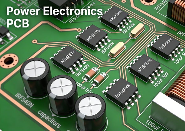
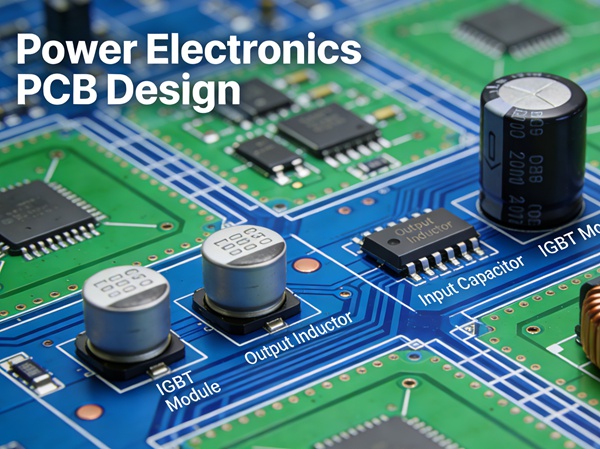
Electric vehicles (EVs) require PCBs capable of handling high currents, high temperatures, and harsh operating environments.
Power electronics PCBs—used in inverters, chargers, and battery management systems—face design challenges that go far beyond standard automotive PCBA:
- High current density traces
- Significant heat generation
- Voltage transients and EMI
- Harsh mechanical and thermal stress
This guide explains best practices for PCB design in EV power electronics, focusing on reliability, thermal performance, and manufacturability.
Table of Contents
Key Design Considerations
1. Copper Thickness and Current Carrying Capacity
High current traces require:
- Increased copper thickness (e.g., 2–5 oz for inverter boards)
- Wider traces for busbars
- Adequate spacing for high voltage
IPC-2221 provides basic current-carrying guidance, but EV applications often require derating for thermal and safety margins.
2. Thermal Management
Power components such as MOSFETs, IGBTs, and diodes generate significant heat.
Design strategies:
- Thermal vias under components to transfer heat to the inner or backside planes
- Large copper pours for heat dissipation
- Thick core substrate for mechanical and thermal stability
- Proper placement of heatsinks and thermal pads
Thermal simulation early in the design ensures hotspot mitigation.
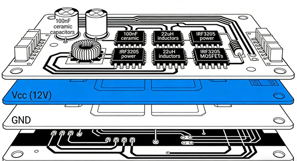
3. Stack-Up Design for Reliability
EV power boards are often multilayer:
- Layer arrangement balances power and signal layers
- Symmetric stack-up reduces warpage during reflow
- Inner planes can serve as ground and thermal planes
- High Tg prepregs required for elevated operating temperatures
Stack-up decisions impact both electrical performance and assembly reliability: PCB Manufacturing Tolerances Explained
4. High Voltage Clearance and Creepage
EV boards often handle hundreds of volts:
- Adequate clearance and creepage per IPC-2221 / ISO 6469 standards
- Conformal coating or insulation for critical areas
- Isolation of high-current and sensitive low-voltage signals
Proper spacing prevents arcing, insulation breakdown, and long-term reliability issues.
5. EMI / Signal Integrity
Power electronics generate high dV/dt and high di/dt:
- Differential pair routing for sensitive signals
- Controlled impedance for high-frequency signals
- Decoupling capacitor placement
- Ground plane segmentation to reduce noise
EMI mitigation ensures controller accuracy and functional safety.
6. PCB Warpage and Assembly Considerations
Large power boards are prone to warpage:
- An uneven copper balance can lead to reflow issues for small control components
- Thermal stress from large MOSFETs and busbars can deform the board
- Controlled lamination and symmetric stack-up improve flatness
See related: PCB Warpage and Reflow Deformation
7. Component Placement for Power Dissipation
Placement strategy:
- High-power components close to heatsinks or metal-core areas
- Minimize thermal path impedance
- Separate sensitive control components from power loops
Proper placement reduces thermal stress and improves reliability.
8. Soldering and Assembly Strategy
High-current pads and thick copper increase thermal mass:
- Requires a modified reflow profile or selective soldering
- Stencil design must accommodate large thermal pads
- Inspection for solder voids under power components is critical
Reference:
BGA Solder Joint Reliability and Failure Analysis Guide
Stencil Design Optimization for SMT Yield
Frequently Asked Questions (FAQ)
A: Depends on current and board size. Commonly 2–5 oz for high-current traces.
A: Use thermal vias, thick copper planes, heatsinks, and thermal simulation to prevent hotspots.
A: High Tg FR-4 or specialized high-temperature laminates are recommended for long-term reliability.
A: Careful layer stack-up, proper decoupling, controlled impedance, and separation of power and sensitive signals.
A: Yes. Proper stack-up, copper balancing, and reflow profile control reduce deformation risk.
Conclusion
Designing PCB for EV power electronics requires:
- High-current trace management
- Thermal performance optimization
- Proper stack-up and material selection
- Voltage isolation and EMI control
- Assembly-aware design
Power electronics PCB design is a system-level engineering task. Early consideration of thermal, electrical, and mechanical factors ensures both high reliability and manufacturability for electric vehicles.