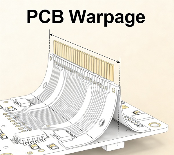
PCB warpage is one of the most underestimated risks in modern electronic manufacturing.
As board density increases and component packages become larger—especially BGA and QFN—board flatness during reflow becomes critical. Even a small deformation can significantly affect solder joint reliability and assembly yield.
This article explains what causes PCB warpage, how it behaves during reflow, how it is measured, and how engineers can reduce risk.
Table of Contents
What Is PCB Warpage?
PCB warpage refers to out-of-plane deformation of the board, either:
- Bow (uniform curvature)
- Twist (diagonal distortion)
- Localized deformation
Warpage may exist before assembly, but it often increases during the thermal stress of reflow soldering.
Flatness at room temperature does not guarantee flatness at peak reflow temperature.
Why Warpage Increases During Reflow
During reflow, PCB temperature typically rises to 230–250°C (lead-free process).
At elevated temperatures:
- Resin softens
- Copper and substrate expand
- CTE mismatch becomes more pronounced
- Internal stress redistributes
If the PCB stack-up is not symmetric, thermal expansion becomes unbalanced, leading to deformation.
This behavior is strongly related to the PCB manufacturing process
Lamination quality and copper distribution directly influence internal stress levels.
Main Causes of PCB Warpage
1. Asymmetric Stack-Up
If layer distribution is uneven (e.g., heavy copper on one side), expansion forces differ across the board thickness.
This creates bending during heating.
Balanced stack-up design is one of the most effective preventive measures.
2. Uneven Copper Distribution
Large copper planes on one side and sparse routing on the other create thermal imbalance.
Copper expands differently from resin, increasing curvature under heat.
Copper balancing techniques reduce this risk.
3. Material CTE Mismatch
Different materials expand at different rates.
Mismatch between:
- Core material
- Prepreg resin
- Copper layers
can amplify deformation during thermal cycling.
4. Large BGA Packages
Large BGA components increase local stress during reflow.
If the PCB surface is not flat, uneven solder collapse can occur, leading to reliability risks discussed in BGA solder joint reliability
5. High Reflow Temperature
Lead-free soldering increases peak temperature compared to leaded processes.
Higher temperature increases expansion and stress.
Excessive soak time can further amplify deformation.
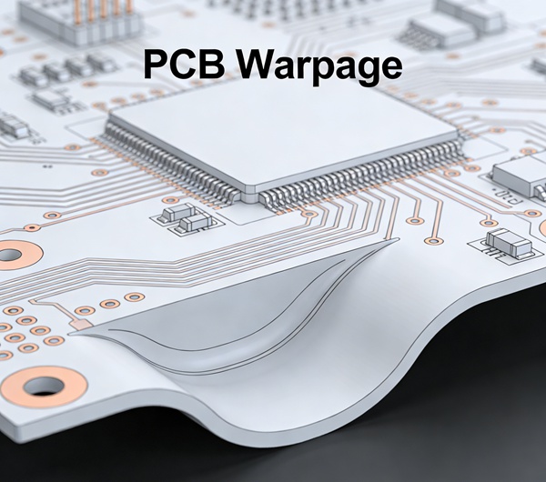
How PCB Warpage Affects Assembly
Warpage can cause:
- Head-in-pillow defects
- Incomplete solder wetting
- Uneven solder joint height
- Increased BGA fatigue risk
- Component misalignment
Even if the board passes electrical testing, deformation during reflow can introduce long-term reliability issues.
Warpage is not just cosmetic—it is a structural reliability concern.
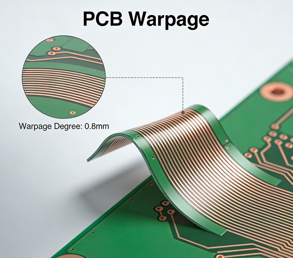
Measuring PCB Warpage
Warpage is typically measured as a percentage: Industry guidelines often limit warpage to around 0.75% or lower for reliable assembly, depending on the application.
Measurement methods include:
- Optical flatness measurement
- Shadow moiré systems
- 3D deformation analysis during thermal cycling
Monitoring deformation at reflow temperature provides more meaningful data than room-temperature measurement alone.
Warpage and PCB Manufacturing Tolerances
Dimensional tolerances influence warpage behavior.
Tight thickness control and balanced lamination reduce deformation risk.
See: pcb manufacturing tolerances
Stack-up design must consider both mechanical and electrical requirements.
Design Strategies to Reduce Warpage
Engineers can reduce risk through:
- Symmetric layer stack-up
- Balanced copper distribution
- Avoiding excessive copper on the outer layers only
- Selecting appropriate Tg materials
- Controlling board thickness
- Reducing panel size when possible
Early DFM review helps identify imbalance before production.
Process Control Strategies During Assembly
Manufacturing controls include:
- Optimized reflow profile
- Controlled heating rate
- Proper support tooling during reflow
- Panel design with sufficient rigidity
Assembly and fabrication must work together to manage deformation.
Warpage in High-Reliability Applications
Automotive and industrial electronics often experience repeated thermal cycling.
Even minor initial deformation can accelerate fatigue cracking over time.
Long-term reliability requires:
- Stable fabrication
- Controlled assembly
- Appropriate material selection
- Validated thermal cycling performance
Frequently Asked Questions (FAQ)
A: Typically below 0.75%, but requirements vary depending on component size and reliability class.
A: Thicker boards generally resist deformation better, but stack-up symmetry and copper balance are more critical than thickness alone.
A: No. Thermal expansion always causes some deformation. The goal is to keep it within acceptable limits.
A: It is both. Fabrication controls internal stress, while the assembly thermal profile influences deformation during reflow.
A: Advanced measurement systems such as shadow moiré allow deformation analysis under controlled heating conditions.
Conclusion
PCB warpage during reflow is a mechanical phenomenon driven by thermal expansion imbalance.
It directly affects BGA reliability, solder joint integrity, and long-term product stability.
Managing warpage requires coordination between PCB design, fabrication control, and assembly process optimization.
Understanding deformation behavior at elevated temperature—not just room temperature—is essential for modern high-density electronics.