Printed Circuit Boards (PCBs) serve as the backbone of modern electronic devices, with their manufacturing advancements directly impacting product performance and reliability. With the rapid development of 5G, IoT, AI, and other cutting-edge technologies, the PCB industry is undergoing unprecedented innovation. This article provides an in-depth analysis of key PCB manufacturing technologies, their applications, and future trends, offering a comprehensive understanding of this specialized field.
Table of Contents
Overview of PCB Manufacturing Processes
PCB manufacturing has evolved from simple single-layer boards to today’s high-density interconnect (HDI) multilayer boards, continuously pushing the limits of physical design. The three primary PCB manufacturing processes are:
Subtractive Process: The most traditional method, where a photoresist is applied to a copper-clad laminate, exposed to create a circuit pattern, and then etched to remove unprotected copper. While mature, this process has limited precision and struggles to meet modern HDI requirements.
Fully Additive Process (SAP): Uses an insulating substrate with a photosensitive catalyst. After selective exposure, copper is chemically deposited only where needed to form circuits. This enables high precision but demands stringent material and process control.
Modified Semi-Additive Process (mSAP): Combines the advantages of subtractive and additive methods. A thin seed layer of copper is chemically deposited, selectively electroplated to thicken circuit traces, and then the excess copper is etched away. This process is ideal for ultra-fine circuitry and has become a mainstream technology for high-end PCBs.
Core Advanced PCB Manufacturing Technologies
Via-in-Pad: Enabling High-Density Interconnects
Via-in-pad technology involves placing conductive vias directly within component pads, significantly improving PCB space utilization.
Key Advantages:
- Saves over 30% board space, ideal for compact designs
- Shortens signal paths, enhancing high-speed circuit performance
- Provides additional thermal pathways, improving heat dissipation for high-power components
Manufacturing Challenges:
- Microvia Drilling: Requires laser drilling for 50–100 μm microvias with ±15 μm positioning accuracy
- Via Filling: Vacuum-assisted resin filling ensures bubble-free voids, with material shrinkage controlled below 2%
- Surface Planarity: Post-filling, precision grinding ensures surface flatness within 5 μm for reliable soldering
- Thermal Stress Management: Filler materials must match copper’s thermal expansion coefficient to prevent cracking
Applications:
- Smartphone motherboards (especially for processors and memory)
- High-end GPUs and server motherboards
- Miniaturized IoT devices
- High-density LED arrays
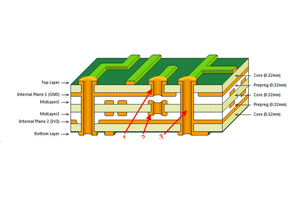
Blind and Buried Vias: 3D Interconnect Solutions
Blind and buried vias enable selective layer connections, allowing three-dimensional PCB routing.
Technology Comparison:
| Type | Structure | Manufacturing Method | Primary Benefit |
|---|---|---|---|
| Blind Via | Connects outer to inner layers | Laser/controlled-depth drilling | Reduces signal stub effects |
| Buried Via | Entirely within inner layers | Laminated after layer processing | Frees up outer-layer routing space |
Key Process Challenges:
- Depth Control: Laser drilling requires precise energy/pulse control (±10 μm tolerance)
- Layer Alignment: High-precision registration systems ensure ≤25 μm misalignment
- Plating Uniformity: Pulse plating ensures even copper deposition (≥18 μm in vias)
- Reliability Testing: Thermal cycling (-55°C to 125°C, 1000 cycles) and impedance testing
Industry Applications:
- 4G/5G base station RF modules
- Aerospace and defense electronics
- Medical equipment control boards
- Autonomous vehicle sensor modules
Modified Semi-Additive Process (mSAP): Ultra-Fine Circuit Fabrication
mSAP uses a “thin seed layer + selective plating” approach to achieve sub-30 μm trace/space, surpassing traditional etching limits.
Process Flow:
- Substrate Prep: Low-roughness base material (Rz < 1.5 μm)
- Seed Layer Deposition: 0.3–1 μm thin copper via electroless plating
- Patterning: Laser Direct Imaging (LDI) with 5 μm resolution
- Plating: Acid copper electroplating (±2 μm thickness control)
- Seed Layer Removal: Micro-etching with <3 μm undercut
Quality Control Metrics:
- Trace width uniformity: CV < 5% across panel
- Copper thickness variation: <10% within board
- Surface defects: <3 defects per m²
Typical Products:
- Smartphone substrate-like PCBs (SLP)
- Wafer-level packaging substrates
- Millimeter-wave antenna arrays
- Ultra-high-density interconnect modules
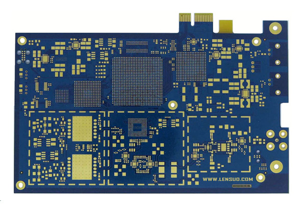
Industry Applications of Advanced PCB Technologies
Consumer Electronics
Smartphones and tablets drive advanced PCB adoption. Flagship smartphone motherboards use any-layer HDI and mSAP to achieve 20/20 μm trace/space rules, packing 14+ layers into 80×120 mm areas. Wearables employ rigid-flex PCBs, maintaining reliability at <3 mm bend radii.
Telecommunications Infrastructure
5G baseband units demand high-frequency PCBs with:
- Dielectric constant (Dk): 3.0±0.05 @ 10 GHz
- Loss tangent (Df): <0.002 @ 10 GHz
- Phase consistency: ±1.5°/inch
These require specialized resin systems and controlled impedance processes.
Automotive Electronics
Autonomous systems impose new requirements:
- Radar PCBs: Ra < 0.3 μm surface roughness for 77 GHz
- Battery management: 6-layer, 2 oz heavy copper boards (8:1 aspect ratio vias)
- Displays: Ultra-thin flexible circuits (>100k bend cycles)
Industrial & Medical Equipment
Industrial controls require:
- 10+ layer power PCBs
- -40°C to 150°C operating range
- Vibration resistance (5–500 Hz, 5 Grms)
Medical imaging relies on:
- Low-noise circuit design
- High-density analog routing
- EMI shielding structures
Future Trends & Technical Challenges
Material Innovations
High-Frequency Materials:
- Modified PTFE composites
- Liquid Crystal Polymer (LCP) films
- Nano-porous silica
Thermal Management:
- >5 W/mK thermal conductivity resins
- Graphene-enhanced substrates
- Insulated metal substrates
Process Breakthroughs
Heterogeneous Integration:
- Embedded passives (>100/cm²)
- Chip-on-Board (COB) technology
- Optoelectronic hybrid circuits
Precision Fabrication:
- Picosecond/femtosecond laser drilling
- Atomic Layer Deposition (ALD) metallization
- Nanoimprint lithography
Sustainability Initiatives
Eco-Friendly Processes:
- Cyanide-free gold plating
- Low-COD electroless copper
- Water-based solder masks
Circular Economy:
- >99.5% copper recovery
- Low-energy manufacturing
- Biodegradable substrates
FAQ: Advanced PCB Manufacturing
Q1: How does via-in-pad improve thermal performance?
A1: Copper-filled vias create thermal pathways, reducing thermal resistance by >40% in 3×3 via arrays. Optimal fill density is 60–70% for thermo-mechanical reliability.
Q2: What are the signal integrity benefits of blind/buried vias?
A2: Compared to through-hole vias, they:
- Shorten signal paths by 30–50%
- Reduce crosstalk by 6–8 dB @ 10 GHz
- Improve impedance matching (15% lower reflection)
- Cut delay by 20–30 ps/inch
Q3: How does MSAP outperform traditional subtractive processes?
A3: Key advantages include:
- Trace width accuracy: ±2 μm vs ±8 μm
- Near-vertical sidewalls (85–90° vs 45–60°)
- Finer geometries (15/15 μm vs 50/50 μm)
- Tighter impedance control (±5% vs ±10%)
Q4: How to evaluate a manufacturer’s blind/buried via capability?
A4: Assess:
- Technical specs (≤50 μm microvias, ±25 μm registration)
- Reliability data (thermal cycling, cross-section analysis)
- Inspection methods (3D X-ray, AOI coverage)
- Production stability (>90% yield at scale)
Q5: What breakthroughs will shape PCB tech in 3–5 years?
A5: Key developments:
- Higher Density: 10/10 μm traces, hybrid mSAP/SAP
- Heterogeneous Integration: Embedded actives/passives, optical interconnects
- Advanced Materials: mmWave low-loss dielectrics (Dk<2.5, Df<0.001)
- Smart Manufacturing: AI-driven optimization, digital twins
- Sustainability: >95% material recycling, 30% energy reduction
As electronics continue advancing toward higher performance, miniaturization, and efficiency, PCB technologies will keep pushing physical limits. Understanding these innovations empowers designers and procurement specialists to make informed decisions, driving next-generation product development.
More related reading
1.PCB Manufacturing Proofing Process
2.PCB Vias
3.High frequency PCB board manufacturing process